R&D Status of FPCCD VTX
Abstract
As a candidate of the vertex detector for experiments at ILC, fully depleted fine pixel CCDs (FPCCDs) are under development. We describe the basic concept of the FPCCD and report on preliminary results of the performance study of the first prototype FPCCD sensors.
1 Introduction
For the vertex detector in ILC experiments, pixel occupancy is one of the most challenging issues. Due to a large amount of electron-positron pairs created by the beam-beam interaction, the pixel occupancy exceeds 10% if the signal is accumulated for one bunch train for pixel detectors with standard () pixel size used for the innermost layer.
In order to reduce the pixel occupancy to an acceptable level (), there are two different approaches studied by several groups. One approach is to readout the signal of the sensors about 20 times per one train. This method requires very fast readout speed and very high peak power during trains. Another approach is to use about 20 times finer pixels of the sensors. In this method, the signal is read out during the train interval of . Therefore, the peak power is quite low. The concept of the fully depleted fine pixel CCD (FPCCD) is an idea to realize the latter approach [2].
2 Development of FPCCD sensors
Our goal of FPCCD R&D is to develop FPCCD sensors with the pixel size of about . In addition to the small size of the pixels, there are several challenges for the FPCCD R&D:
- (1)
The sensors have to be fully depleted to suppress the charge spread due to diffusion.
- (2)
Because very small signal ( electrons) is expected for an inclined track traversing a pixel, the noise level of the sensor should be less than 50 electrons.
- (3)
Readout speed should be Mpixel/s to reduce charge transfer inefficiency.
- (4)
Power consumption (mainly by the output circuit) should be mW/channel in order to keep the detector system at with a gentle air (cool gas) flow.
- (5)
Horizontal register as small as the pixels has to be put in the image area.
- (6)
Wafer thickness should be as thin as m to suppress the multiple scattering.
Multi-port readout of a sensor is indispensable to read out a large number of pixels in 200 ms. There are two options for multi-port readout as shown in Figure 1.

In the option shown in Figure 1(a), which was adopted for the CCD sensors used for the vertex detector of SLD, the number of vertical (parallel) transfer of the charge is larger than that of horizontal (serial) transfer. On the other hand, the number of horizontal transfer is larger than that of vertical transfer in the option shown in Figure 1(b). Our FPCCD design is based on the option (b) from the view point of radiation tolerance (CTE:charge transfer efficiency). Charge transfer inefficiency (CTI) due to traps caused by radiation damage becomes smaller if , where is electron capture time constant ( for 0.42 eV level). For horizontal transfer clock frequency of MHz and vertical transfer clock frequency of MHz, the CTI associated with the vertical transfer is larger than the CTI of horizontal transfer. Therefore, smaller number of vertical shift realized in the option (b) is more advantageous. The horizontal register in option (b) has to be put in the image area while keeping sensitivity to charged tracks.
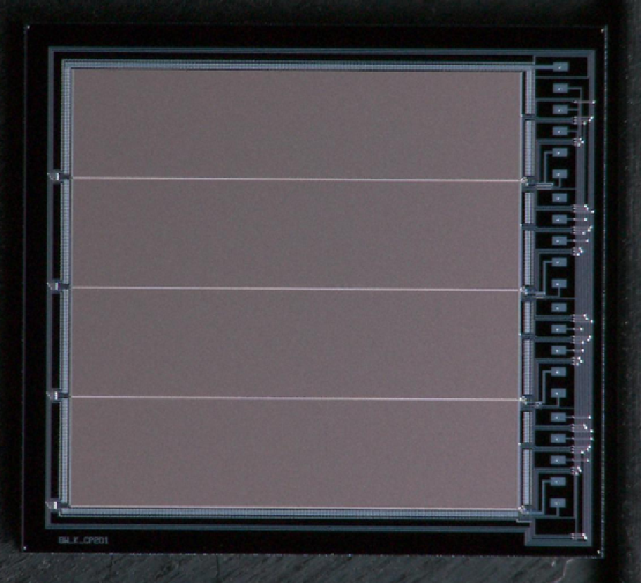
We have already succeeded to develop fully-depleted CCDs (the item (1) in the list above) by using high resistivity epitaxial layer [3]. In order to tackle the challenges of (2)–(5) among the issues listed above, we have fabricated the first prototype FPCCD sensors collaborating with Hamamatsu Photonics. The sensors are delivered in packaged shape and as bare chips (see Figure 2). The pixel size is m square in this prototype. Each chip has pixels and is read out through four readout ports. White lines seen in the image area in Figure 2 correspond to horizontal registers.
Several variants of FPCCD sensors have been manufactured. The sensor has several different designs of the output amplifier. Two types of wafers with the epitaxial-layer thickness of m and m are used. For the gate oxide layer of the output transistors, two types of chips with standard thickness and thin type are produced.
3 Characteristics of prototype sensors
Basic characteristics of the prototype FPCCD sensors are measured by the manufacturer with the operating condition of , k, readout frequency of 10 MHz at room temperature. The output gain and the power consumption of the output amplifier are 5.2–6.9 V/electron and 10–15 mW/channel, respectively, depending on the design of the amplifier.

We have tested the prototype sensors using line-focused laser light at KEK. Figure 3 shows a close-up image of the line-focused laser near the horizontal register taken by a prototype FPCCD sensor. The first (bottom) line corresponds to the horizontal register. It can be seen that the horizontal register is sensitive to light. Actually, the signal of the horizontal register is significantly smaller than standard pixels because the horizontal register is partially covered by aluminum layer for gate clocking.
In the prototype FPCCDs, large dark current on both horizontal edges was observed. Another problem of charge injection into first few tens of pixels of first few tens of lines was found when vertical clock is held “high” for 20 ms before reading out a frame. In the next batch of prototype in 2009, the latter problem is expected to be resolved. In addition, increased full-well capacity is planned to be achieved in the next prototype.
Acknowlegements
This work is partly supported by Grant-in-Aid for Scientific Research No. 17540282 and No. 18GS0202 from Japan Society for the Promotion of Science (JSPS), and No. 17043010 and No. 18034007 from Ministry of Education and Science in Japan.
References
- [1]
Presentation:
http://ilcagenda.linearcollider.org/contributionDisplay.py?contribId=162&sessionId=21&confId=2628 - [2] Y. Sugimoto, Proceedings of International Linear Collider Workshop LCWS05, Stanford, CA, March 2005, 550–554.
- [3] Y. Sugimoto, Proceedings of International Linear Collider Workshop LCWS2007, DESY, Hamburg, May 2007, 483–485.