Screening of electromagnetic field fluctuations by –wave and –wave superconductors
Abstract
We investigate theoretically the shielding of the electromagnetic field fluctuations by –wave and –wave superconductors within the framework of macroscopic quantum electrodynamics. The spin flip lifetime is evaluated above a niobium and a bismuth strontium calcium copper oxide (BSCCO) surface, and the screening effect is studied as a function of the thickness of the superconducting layer. Further, we study the different temperature dependence of the atomic spin relaxation above the two superconductors.
pacs
34.50.+a, 03.75.Be, 74.40.+k, 74.72.-hI Introduction
Recent advances in the trapping of neutral atoms near microstructured surfaces [1, 2], colloquially referred to as atom chips, has proved these structures to be promising for the coherent manipulation of cold atom clouds. Applications of atom chips include the imaging of the electromagnetic field near metallic and dielectric surfaces [3, 4], the accurate measurement of gravity [5, 6] and atom interferometry [7, 8]. One of the central challenges proves to be the interaction between the trapped atoms and the hot surfaces in their vicinity, which leads to thermally-induced spin relaxation dynamics and attractive Casimir–Polder forces. The atomic lifetime is limited by the transitions between trapped and untrapped states induced by fluctuating electromagnetic fields arising in conducting materials [9, 10].
The origin of the electromagnetic field fluctuations lies in the finite resistivity (and the finite temperature) of conducting materials as a consequence of the fluctuation-dissipation theorem. Superconductors have a (almost) negligible resistivity and their thermal fluctuations are attenuated with respect to a dielectric or a metal. An important enhancement of the atomic lifetime is expected with the adoption of superconducting surfaces, and both theoretical and experimental investigations have recently turned their attention to superconducting materials [11, 12, 13, 14, 15, 16, 17].
In this article, we investigate the shielding of the near-field noise in the vicinity of a dielectric substrate provided by two different superconducting films. Casimir–Polder potential and thermally induced spin flips are among the effects which may be altered when a superconducting layer is placed above a dielectric structure, and we will focus on the latter.
Previous theoretical investigations on superconducting atom chips have been concerned with the increase of the spin flip lifetime and vortex detection via spin dynamics [11, 14]. Three different descriptions of superconductivity have been adopted to estimate the spin flip rate [18]: the two-fluid model, the Bardeen–Cooper–Schrieffer (BCS) theory and the Eliashberg theory. The Eliashberg theory provides the most appropriate model for the electromagnetic energy dissipation in superconducting materials, whereas the other two theories ignore the strong modification of either the imaginary part or the real part of the optical conductivity in the superconducting state. Nevertheless, the spin flip lifetime evaluated with the two-fluid model gives remarkably accurate estimates of the Eliashberg results [18].
Quantum mechanical approaches for spin flip lifetime calculations above superconducting atom chips have considered only isotropic conventional (-wave) superconductors. In this paper we introduce a comparison between the screening properties of a conventional -wave superconductor such as niobium, and an unconventional -wave superconductor such as bismuth strontium calcium copper oxide (BSCCO). The main difference between these two classes of materials is the way in which the electrons interact with each other to form Cooper pairs [19]. In conventional -wave superconductors, the two electrons of a Cooper pair are in a state with zero total spin and total angular momentum, such that their state is isotropic and the superconducting phase is homogeneous with an uniform penetration depth .
In -wave superconductors, an unconventional pairing takes place and the state of the paired electrons has a zero total spin while the total angular momentum is (hence the name). Such superconducting state is anisotropic giving rise to layered superconductors, which are characterised by an anisotropic permittivity. This results from the in-plane penetration depth being different from the longitudinal penetration depth .
As an example, we report the values of the penetration depth for the two superconducting materials considered in this work. For zero temperature, niobium has a penetration depth of nm [20], whereas the transverse and in plane penetration depth of BSCCO are m and nm, respectively [21].
Furthermore, -wave superconductors have rather high transition temperatures. For example, for BSCCO one finds transition temperatures of up to K while for thin niobium films one has K (compared to K for bulk niobium). The origin lies in the crystal structure of unconventional superconductors [19]. The interlayers act as a reservoir of charge carriers that combine into Cooper pairs and, depending on the concentrations of oxygen atoms into the material, the transition temperature increases from small values up to a maximum value of 90 K.
Not only the value of the transition temperature, but also the temperature dependence of the penetration depth differs in both types. In conventional superconductors, the deviation of the penetration depth from its value at can be approximated by the empirical formula [19]
| (1) |
while in -wave superconductors, increases with as [19, 22]
| (2) |
In present experiments on superconducting atom chips, the superconductor is deposited on an insulator, as its contact with a metal can perturb the superconducting properties. However, in order to emphasize the screening properties of a superconducting medium, we consider the superconducting film to be ideally placed above a metal substrate. We emphasize here that all the results obtained are valid only for the superconductors in the Meissner state. The Meissner state is observed when a magnetic field in any point of a superconductor is below the first critical field, which is 140 mT for niobium and 13 mT for BSCC0 at 4.2 K. In an higher field, the magnetic field penetrates into the superconductor (type-II) in the form of vortices. In this so-called mixed state a superconductor exhibits different screening properties and dependences on frequency and temperature from the Meissner state, hence the results presented here are not valid for the mixed state.
The paper is organized as follows. In Sec. II, we give a brief introduction into vacuum fluctuation effects with emphasis on spin flip transitions and the Lamb shift. The expressions for the spin flip rate in isotropic and anisotropic planar multilayered structures is discussed in detail in Sec. II.1 and in the Appendix. The results on atomic spin relaxation are given in Sec. III with the screening properties investigated in Sec. III.1 and the temperature dependence of the penetration depth investigated in Sec. III.2. Our conclusions are given in Sec. IV.
II Vacuum fluctuations
The spontaneous decay of an excited atom is one of the most widely studied effects of the ground-state fluctuations of the electromagnetic vacuum [23]. However, the presence of a dielectric or metallic body strongly modifies the vacuum field and its statistical properties [24], leading to a modification of the spontaneous emission rate as well as the Lamb shift. In particular, the latter is associated with the appearance of an attractive dispersion force, the Casimir–Polder force. The energy shift is position-dependent and takes the form of , where the first term is the contribution to the Lamb shift in free space, while the second term is the position-dependent van der Waals potential of an atom at position . Another related issue associated to the modification of the vacuum field is the body-induced modification of the atomic spin flip lifetime [10], which is the main subject of this paper.
Due to the Meissner effect, the presence of a superconducting material provide a shield for the field fluctuations arising from a conducting substrate. The energy gap of a superconductor is , with the Boltzmann constant, and corresponds to the minimum excitation energy required to break a Cooper pair. In -wave superconductors, the gap frequency is almost of the order of THz (e.g. GHz for niobium [25]), while in -wave superconductors it is usually an order of magnitude larger due to the higher transition temperature (e.g. the BSCCO gap frequency is given in the literature as 7.5 THz [26]). All the physical phenomena resulting from field fluctuations are going to be attenuated as long as the range of frequencies involved are smaller than the gap frequency.
The atomic spin flip lifetime is enhanced by the presence of a superconductor as the typical transition frequencies are of the order of MHz and fall well below the gap frequency for both -wave and -wave superconductors. The same cannot be said straightaway for the van der Waals potential. The induced energy shift and broadening results in the atom having a position-dependent polarizability associated with the relevant dipole transitions of the atom. The potential is given by the sum of two terms: a contribution resonant with the magnetic dipole transitions and an off-resonant contribution [27]. For an atom in its ground state, the resonant term vanishes and the off-resonant term is obtained by integrating over all the frequencies, which means that an attenuation of the potential for frequencies is not relevant on the overall effect. Hence, the Casimir–Polder force experienced by a ground state atom is largely unaffected by the presence of either -wave or -wave superconductors. However, the resonant term may dominate for an atom in an excited state and a superconductor may play a significant role. Typical optical transition frequencies for an atom are of the order of THz, and -wave superconductors in principle may be able to alter their Casimir–Polder potential.
II.1 Spin flip rate
The spin flip rate of an atom placed near a conducting or superconducting body is obtained within the formalism of macroscopic quantum electrodynamics as [10]
| (3) | |||||
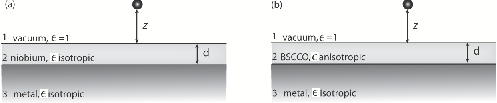
where is the spin matrix element for the relevant transition, denotes the Bohr magneton, and is the electron’s factor. The Green function is the fundamental solution to the classical Helmholtz equation and thus contains all necessary geometric and electromagnetic information about the macroscopic bodies. We review in the Appendix how to evaluate the Green tensor for an anisotropic multilayered planar structure such as the one represented in Fig. 1 consisting of vacuum, superconducting layer and metal substrate.
The spin flip rate for a planar multilayered structure made of isotropic layers is known to be [28]
| (4) |
where the spin matrix elements have been evaluated for the 87Rb ground state transition between the magnetic hyperfine sublevels . Let us recall here that Eq. (4) is valid whenever the atomic transition wavelength can be regarded as the largest wavelength of the system. The generalized Fresnel reflection coefficient for a three-layer geometry reads
| (5) |
where is the thickness of layer 2. The function is the Fresnel reflection coefficient for TE waves at a planar interface defined as
| (6) |
with and with the label indicating the layer. The coefficient has the same form as after the replacements and have been made.
The dielectric function for a normal metal is given by where is the skin depth of the metal and . In the two-fluid model [19], the dielectric function of a superconductor can be written as
| (7) |
where and are the skin depth and the conductivity associated with the normally conducting electrons, respectively. The optical conductivity corresponding to Eq. (7) is
| (8) |
Both the penetration depth and the skin depth are temperature dependent [19],
| (9) |
where is the electrical conductivity of the metal in the normally conducting state for , and and are the electron densities of the superconducting and normal state, respectively, at a temperature . The total electron density is constant, with for and for . It follows from Eq. (1) that Eq. (9) can be written as
| (10) |
with for an -wave superconductor, and for a -wave superconductor.
In contrast, in a -wave superconductor the penetration depth and thus the permittivity is highly anisotropic so that it can be written as a tensor of the form
| (11) |
where and are the transverse and longitudinal scalar permittivities of the layer corresponding to and , respectively. We calculate the spin flip rate for the BSCCO structure as
| (12) |
where and are the relevant scattering coefficients given in the Appendix. We assume that the whole structure of metallic substrate plus superconductor is in thermal equilibrium with its surroundings. The electromagnetic field is then in a thermal state with temperature , equal to the temperature of the materials. Therefore, both spin flip rates in Eq. (4) and Eq. (12) need to be multiplied by a factor where the mean thermal photon number is
| (13) |
III Atomic spin relaxation
In this section, we study the atomic spin relaxation above a niobium and a BSCCO surface. We imagine that a 87Rb atom is held at a distance from the superconducting surface as shown in Fig. 1. The spin flip lifetime is evaluated for the 87Rb ground-state transition with the transition frequency taken to be kHz. The comparison between niobium and BSCCO is done in terms of the screening of the electromagnetic field fluctuations affecting the atomic spin dynamics. Further comparison is done by studying the temperature dependence of the spin flip lifetime.
III.1 Screening
The alteration of the spin flip lifetime as a function of the relevant length scales of the system is an indication of the capabilities of niobium and BSCCO to screen the electromagnetic field fluctuations that arise from the underlying metal substrate. We consider the multilayered structures as represented in Fig. 1 and we plot the atomic spin flip lifetime as a function of the distance from the surface in Fig. 2. Two different thicknesses of the superconducting layer are taken into consideration.
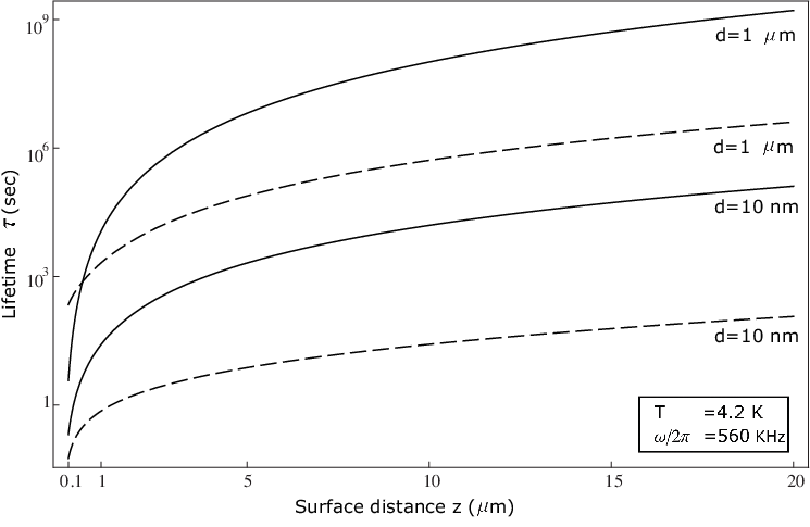
For both niobium and BSCCO, the lifetime increases with the thickness of the superconducting layer, and the longest lifetimes are obtained for the atom trapped above niobium (continuous line in Fig. 2). During the superconducting phase, magnetic field lines are expelled from the material except for a thin surface layer (with thickness of the order of the penetration depth), where shielding currents flow. Therefore, fluctuating magnetic fields are attenuated by the shielding currents. We now define a screening factor as a function of the thickness of the superconducting layer as
| (14) |
where is the spin flip lifetime associated with the bare copper substrate obtained by combining Eq. (4) and Eq. (6).
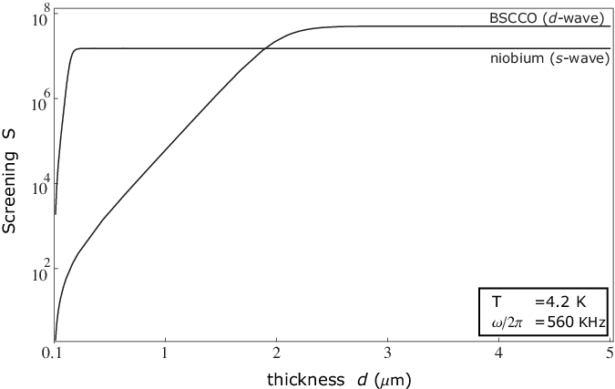
This screening factor is plotted in Fig. 3 for niobium and BSCCO films and for an atom held at a fixed m distance from the surface. The screening increases in both structures for thicknesses roughly the same size as the penetration depths at zero temperature (recall that nm for niobium and m for BSCCO). For a superconducting layer that is thicker that the corresponding penetration depth, the screening effect saturates which confirms the fact that only the penetration depth provides an active screening of the electromagnetic field fluctuations as already seen for dielectrics [11, 28].
We emphasize that the results presented in this paragraph are only indicative for the two superconducting structures. The superconducting properties change both with the layer thickness being less than the coherence length (i.e. 30 nm for niobium at 4K).
III.2 Temperature dependence
Let us now investigate the temperature dependence of the spin flip lifetime. We have chosen a different thickness for each of the superconductors: m for niobium and m for BSSCO, corresponding to the thickness providing the maximum screening (see Fig. 3). As shown in Eq. (1) and Eq. (2), the penetration depth is a function of the temperature, which is reflected in the temperature dependence of the optical conductivity in Eq. (8). However, the spin flip lifetime is proportional to the mean thermal photon number , , which may become dominant for large enough temperatures.
The comparison is carried out in two stages. First, in Fig. 4 we show the lifetime as a function of temperature, while in Fig. 5 we show as a function of , in order to study how the different power laws affect the lifetimes near the transition temperature.

The inset in Fig. 4 shows the spin flip lifetime for temperatures where both niobium and BSCCO are superconducting. The lifetime near superconducting niobium is several orders of magnitude larger than near superconducting BSSCO. In particular, at the liquid helium temperature K, the two lifetimes are approximately s and s as shown in the inset of Fig. 4. At the liquid nitrogen temperature K, only BSCCO is still in the superconducting phase giving a lifetime of roughly s, while the lifetime above (normally conducting) niobium is estimated to be s.

In Fig. 5, the spin flip lifetime is plotted as a function of based on Eqs. (4) and (12). For temperatures , we neglect the dependence of the permittivity in Eq. (7) as . For , the lifetime above BSCCO decreases with a smaller power law compared to niobium as a results of the penetration depth dependence on temperature. There is a marked difference in the transition from the normal state to the superconducting state, and we expect this to be visible in experiments comparing the two structures considered here. According to our results, the temperature dependence of the permittivity in -wave and -wave superconductor can then be tested by observing the atomic relaxation rate near the transition temperature.
We would like to draw the attention to the orientation of the atomic spin and how the spin flip rate changes according to it. The results presented in this section have been obtained for a randomly oriented spin. Due to the anisotropic permittivity of BSCCO, the shielding of the electromagnetic field fluctuations can in principle be different depending on which component couples to the atomic spin. However, our estimates of the spin flip lifetime for a spin oriented either perpendicular or parallel to the interface suggest that the difference is not very pronounced. In fact, the spin flip lifetimes for the two orientations differ only for a factor of 2, the parallel orientation giving the longer lifetime, and it does not depend on the anisotropic permittivity. This indicates that, despite the transverse penetration depth being of the same order of magnitude as in metals, electromagnetic field fluctuations are shielded by screening currents independently from the anisotropy.
IV Conclusion
We have considered the shielding of the electromagnetic field fluctuations provided by a superconductor. The modification of the vacuum field and its properties in the vicinity of a dielectric leads to the appearance of the Casimir–Polder potential and thermally-induced spin flip transitions. The frequencies associated with these two phenomena are very different and only when they fall below the superconducting gap frequency, the presence of the superconducting material is detectable. While the frequencies associated with spin transitions are always smaller than the gap frequency, the same can not be said for the frequencies involved in the Casimir–Polder potential and numerical calculations need to be done.
In this paper we have focused on the atomic spin relaxation above a niobium and a BSCCO surface. We have chosen these two materials as representatives of an -wave and a (high-temperature) -wave superconductor, respectively. We have considered a planar multilayered structure with the respective superconducting layer placed above a copper substrate. The shielding properties of the two superconductors have been investigated by defining a screening factor for the atomic spin relaxation and studying its dependence on the thickness of the superconducting layer. Despite not having obtained an analytical solution, we can still affirm that there is an active screening in the penetration depth layer of the superconductors. When the thickness is bigger than the penetration depth, the screening saturates. We believe that these results represent an important step towards the adoption of neutral atoms as sensitive probes in the study of properties of different types of superconductors.
The temperature dependence of the permittivity in -wave and -wave superconductor follows two different power laws, such difference has been studied by comparing the spin flip lifetime. When both niobium and BSCCO are in the superconducting phase, the niobium gives the longest lifetimes. The comparison has been carried on by investigating the spin flip lifetime near the superconducting transition. There is a marked difference between the two superconductors for , which we believe can be observed experimentally to test the different temperature dependences.
Acknowledgements.
This work was supported by the UK Engineering and Physical Sciences Research Council (EPSRC), the UK Quantum Information Processing Interdisciplinary Research Collaboration (QIP IRC), and the SCALA programme of the European commission.Appendix A Green function for anisotropic planar multilayers
In this section, we present our calculation of the Green tensor for an anisotropic multilayered structure based on the work of Li et al. in Ref. [29]. The geometry of the problem is shown in Fig. 1b where the second layer is characterized by a tensor dielectric permittivity as in Eq. (11). The Green function will be expressed in terms of an expansion of the cylindrical vector wave functions adopting the cylindric basis . For an atom located at in the first layer (vacuum), the Green tensor can be written as
| (15) |
where is the unbounded (bulk) Green tensor representing the contribution of direct waves from the source at to the point , while describes the reflection of waves from the interface between the first and second layer.
The unbounded Green function can be written as
| (16) | |||||
with and . The scattering dyadic Green function has a form similar to the unbounded Green function and can be formulated as
| (17) | |||||
where in the th layer with
| (18) | |||||
| (19) |
and . The cylindrical vector wave functions are defined as
| (20) | |||||
| (21) |
in which is the Bessel function of the first kind and the first order, and is generally defined as .
The coefficients , and are determined by satisfying the boundary conditions for the Green function at the interface between layers. For the sake of simplicity, we are now going to choose a reference system such that the coordinate can be safely set equal to 0 and the Bessel functions can be expanded for such that and
The spin flip rate as in Eq. (3) has been evaluated throughout this paper for a randomly oriented spin. We consider the relaxation rate to be the sum of the contribution given by the atomic spin parallel or perpendicular to the planar substrate. We calculate the double curl of the Green function such that , with the component coupling to the parallel orientation of the spin and the components coupling to the spin perpendicularly oriented. The double curl of the scattering Green tensor reads
| (22) | |||||
The scattering coefficients for a general argument are given by
| (23) | |||||
with
| (24) | |||||
| (25) |
where is the height of the second layer, and and are the weighting coefficient that in our case equal to 1. To obtain the specific scattering coefficients, has to be substituted by or .
References
- [1] C. Henkel, J. Schmiedmayer, and C. Westbrook, Euro. Phys. J. D 35, 1 (2005) and following articles.
- [2] J. Fortágh and C. Zimmermann, Rev. Mod. Phys. 79, 1 (2007).
- [3] S. Wildermuth, S. Hofferberth, I. Lesanovsky, E. Haller, L.M. Andersson, S. Groth, I. Bar-Joseph, P. Krüger, and J. Schmiedmayer, Nature (London) 435, 440 (2005).
- [4] B. V. Hall, S. Whitlock, R. Anderson, P. Hannaford, and A. I. Sidorov, Phys. Rev Lett. 98, 030402 (2007).
- [5] P. Cláde, S. Guellati–Khélifa, C. Schwob, F. Nez, L. Julien, and F. Biraben, Europhys. Lett. 71, pp. 730–736 (2005).
- [6] G. Ferrari, N. Poli, F. Sorrentino, and G.M. Tino, Phys. Rev Lett. 97, 060402 (2006).
- [7] T. Schumm, S. Hofferberth, L. M. Andersson, S. Wildermuth, S. Groth, I. Bar–Joseph, J. Schmiedmayer, and P. Kruger, Nat. Phys. 1, 57 (2005).
- [8] A. Günther, S. Kraft, C. Zimmerman, and J. Fortágh, Phys. Rev. Lett. 98, 140403 (2007).
- [9] M.P.A. Jones, C.J. Vale, D. Sahagun, B.V. Hall, and E.A. Hinds, Phys. Rev. Lett. 91, 080401 (2003).
- [10] P.K. Rekdal, S. Scheel, P.L. Knight, and E.A. Hinds, Phys. Rev. A 70, 013811 (2004).
- [11] S. Scheel, P.K. Rekdal, P.L. Knight, and E.A. Hinds, Phys. Rev. A 72, 042901 (2005).
- [12] T. Nirrengarten, A. Qarry, C. Roux, A. Emmert, G. Nogues, M. Brune, J.-M. Raimond, and S. Haroche, Phys. Rev. Lett. 97, 200405 (2006).
- [13] T. Mukai, C. Hufnagel, A. Kasper, T. Meno, A. Tsukada, K. Semba, and F. Shimizu, Phys. Rev. Lett. 98, 260407 (2007).
- [14] S. Scheel, R. Fermani, and E.A. Hinds, Phys. Rev. A 75, 064901 (2007).
- [15] T. Müller, X. Wu, A. Mohan, A. Eyvazov, Y. Wu, and R. Dumke, New J. Phys. 10, 073006 (2008).
- [16] V. Dikovsky, V. Sokolovsky, Bo Zhang, C. Henkel, and R. Folman, Eur. Phys. J. D 51, 247Ð259 (2009).
- [17] D. Cano, B. Kasch, H. Hattermann, D. Koelle, R. Kleiner, C. Zimmermann, and J. Fortgh, Phys. Rev. Lett. 101, 183006 (2008).
- [18] U. Hohenester, A. Eiguren, S. Scheel, and E.A. Hinds, Phys. Rev. A 76, 033618 (2007).
- [19] W. Buckel and R. Kleiner, Superconductivity, Fundamentals and Applications (Wiley-VCH, Weinheim, 2004).
- [20] P. B. Miller, Phys. Rev. 113, 1209 (1959).
- [21] R. Kleiner and P. Müller, Phys. Rev. B 49, 1327 (1994).
- [22] I. Bonalde, Microelec. J. 36, 907-912 (2005).
- [23] P.W. Milonni, The quantum vacuum: An introduction to quantum electrodynamics (Academic Press, London, 1994).
- [24] S. Scheel and S.Y. Buhmann, Acta Phys. Slov. 58, 675 (2008).
- [25] N.N. Iosad, A. V. Mijiritskii, V. V. Roddatis, N. M. van der Pers, B. D. Jackson, J. R. Gao, S. N. Polyakov, P. N. Dmitriev, and T. M. Klapwijk, J. Appl. Phys. 88, 5756 (2000).
- [26] M.M. Doria, F.M.R. Almeida, O. Buisson, Phys. Rev. B 57, 5489 (1998).
- [27] S.Y. Buhmann and S. Scheel, Phys. Rev. Lett. 100, 253201 (2008).
- [28] R. Fermani, S. Scheel, and P.L. Knight, Phys. Rev. A 73, 032902 (2006).
- [29] L.-W. Li, J.-H. Koh, T.-S. Yeo, M.-S. Leong, and P.-S. Kooi, IEEE Trans. Antennas Propagat. 52, 466 (2004).