Transport, magnetic, and structural properties of La0.7Ce0.3MnO3 thin films. Evidence for hole-doping
Abstract
Cerium-doped manganite thin films were grown epitaxially by pulsed laser deposition at C and oxygen pressure Pa and were subjected to different annealing steps. According to x-ray diffraction (XRD) data, the formation of CeO2 as a secondary phase could be avoided for Pa. However, transmission electron microscopy shows the presence of CeO2 nanoclusters, even in those films which appear to be single phase in XRD. With O2 annealing, the metal-to-insulator transition temperature increases, while the saturation magnetization decreases and stays well below the theoretical value for electron-doped La0.7Ce0.3MnO3 with mixed Mn3+/Mn2+ valences. The same trend is observed with decreasing film thickness from 100 to 20 nm, indicating a higher oxygen content for thinner films. Hall measurements on a film which shows a metal-to-insulator transition clearly reveal holes as dominating charge carriers. Combining data from x-ray photoemission spectroscopy, for determination of the oxygen content, and x-ray absorption spectroscopy (XAS), for determination of the hole concentration and cation valences, we find that with increasing oxygen content the hole concentration increases and Mn valences are shifted from 2+ to 4+. The dominating Mn valences in the films are Mn3+ and Mn4+, and only a small amount of Mn2+ ions can be observed by XAS. Mn2+ and Ce4+ XAS signals obtained in surface-sensitive total electron yield mode are strongly reduced in the bulk-sensitive fluorescence mode, which indicates hole-doping in the bulk for those films which do show a metal-to-insulator transition.
pacs
75.47.Lx,72.60.+g,71.30.+h,61.05.cj,68.37.Lp,81.15.FgI Introduction
Hole-doped manganese perovskite oxides LaMnO3, where is a divalent alkaline earth metal, have been intensively studied over the last years due to the interesting interplay between charge, spin, orbital and structural degrees of freedom.[1, 2, 3] Without doping, LaMnO3 is an antiferromagnetic insulator due to the super-exchange between the Mn3+ ions.[4] In the hole-doped manganites, the divalent ion introduces holes by changing some Mn valences from Mn3+ to Mn4+. The properties of the hole-doped manganites are determined by the interplay of Hund´s rule coupling and the Jahn-Teller distortion of the Mn3+ ions.[5] Their behavior can be qualitatively described by the double-exchange model,[6, 7] describing the interaction between manganese ions with mixed valences (Mn3+ and Mn4+). The strong spin-charge coupling via the double-exchange interaction explains the correlation between the metal-to-insulator (MI) and ferromagnet-to-paramagnet (FP) transition. Close to the MI transition temperature an external magnetic field can reduce the spin disorder and therefore enhance the electron hopping between the manganese ions with mixed valences. This results in a large resistivity drop, called colossal magnetoresistance.[8]
By substitution of La with a tetravalent ion, like Ce,[9, 10, 11] Sn,[12] or Te,[13] instead of a divalent one, some of the Mn3+ ions become Mn2+ with electronic structure te (compared to the te electronic structure for Mn3+). Hence, an extra electron may be induced in the eg-band. Since Mn2+ is a non-Jahn-Teller ion, like Mn4+, one might expect a similar magnetic interaction between the Mn3+ and Mn2+ ions as for the well known hole-doped case.[14]
The first attempts to achieve electron-doping by substituting La with Ce were reported by Mandal and Das.[9] However, they found hole-doping in their bulk samples. Later on, it was revealed that the bulk samples are a multiphase mixture which leads to the hole-doped behavior.[11, 15] Single phase La0.7Ce0.3MnO3 (LCeMO) thin films have been prepared without any CeO2 impurities [16, 17] regarding x-ray diffraction (XRD) data. The films showed FP and MI transitions similar to the hole-doped manganites. Surface-sensitive X-ray photoemission spectroscopy revealed the existence of Mn2+ and Mn3+ valences,[14, 18] which was interpreted as evidence of electron-doping. However, Hall measurements and thermopower measurements on comparable samples showed a hole-type character. [19, 20, 21, 22] By Ganguly et al. [11] it was further questioned whether LaMnO3 accepts Ce-doping at all. Those authors questioned the reports on single phase LCeMO-films and claimed the presence of multi-phase mixtures, consisting of hole doped La-deficient phases with cerium oxide inclusions. Certainly, the existence of electron-doped manganites could enable new types of spintronic devices, such as junctions based on doped manganites.[23] This motivates further research in order to improve understanding of the basic properties of those materials.
In this paper we present the results of studies on transport, magnetic and structural properties of LCeMO thin films grown by pulsed laser deposition (PLD) and their dependence on deposition parameters, annealing procedures and film thickness. We combine a variety of different characterization techniques in order to clarify the nature of the FP and MI transition in our LCeMO thin films.
II Experimental Details
A commercially available stoichiometric polycrystalline La0.7Ce0.3MnO3 target was used for thin film growth by PLD on (001) SrTiO3 (STO) substrates (unless stated otherwise). The target was ablated by using a KrF ( = 248 nm) excimer laser at a repetition rate of Hz. The energy density on the target was , while the substrate temperature during deposition was kept at C for all films for which data are presented below, except for sample K with slightly lower and (cf. Tab. 1). The oxygen pressure during film growth was varied in the 1–25 Pa range with the aim of yielding single phase films with optimum morphology. We used a relatively low deposition pressure as compared to some literature data [14, 19, 23, 24] in order to avoid over-oxygenation of the films. This is important, as it is known that perovskite rare-earth manganites can accept a large excess of oxygen via the formation of cation vacancies, inducing hole-doping in the parent compound LaMnO3.[25] In-situ high-pressure reflection high energy electron diffraction (RHEED) was used to monitor the growth mode and film thickness. After deposition, most of the films were in-situ annealed for 1 h at C and bar and then cooled down with 10∘C per minute. In the following, those samples will be called ”in-situ annealed“ films, in contrast to the ”as-deposited“ films which were just cooled down to room temperature under deposition pressure. Some of the samples have been additionally annealed ex-situ at bar in one or two steps ( step at C; step at C; each step for one hour). Table 1 summarizes the fabrication conditions and some characteristics of the LCeMO films described below.
| # | (Pa) | annealing | (nm) | -axis () | (K) | |
|---|---|---|---|---|---|---|
| in-situ | ex-situ | |||||
| A | 1 | no | no | 100 | 3.921 | – |
| B1 | no | 3.905 | 175 | |||
| B2 | 3 | no | 90 | – | 250 | |
| C | 8 | yes | no | 100 | 3.897 | 190 |
| D | 25 | no | no | 100 | 3.880 | 180 |
| E1 | no | 3.894 | 210 | |||
| E2 | 8 | yes | 65 | 3.887 | 216 | |
| E3 | 3.872 | 230 | ||||
| F | 8 | yes | no | 40 | 3.879 | 223 |
| G | 8 | yes | no | 20 | 3.870 | 232 |
| H | 3 | no | 100 | 3.876 | 260 | |
| K | 3 | no | no | 50 | 3.894 | 180 |
Cooled in 1 bar O2 without 1 hour in-situ annealing
deposited at C with
The surface morphology was checked by atomic force microscopy (AFM) in contact mode. The crystal structure of the films was characterized by XRD and by high-resolution (HR) transmission electron microscopy (TEM). Transport properties were measured with a four probe technique, and a superconducting quantum interference device (SQUID) magnetometer was used to determine the magnetic properties of the samples. Hall measurements were performed in order to obtain information on the dominating type of charge carriers, and x-ray photoemission spectroscopy (XPS) was performed in order to obtain information on the oxygen content of different samples. The valences of the manganese and cerium ions were evaluated by x-ray absorption spectroscopy (XAS). XAS measurements in surface-sensitive total electron yield (TEY) mode and bulk sensitive fluorescence yield (FY) mode were carried out at the WERA dipole beamline (ANKA, Karlsruhe, Germany) with typical energy resolutions set between 100 and 400 meV.
III Structural Analysis
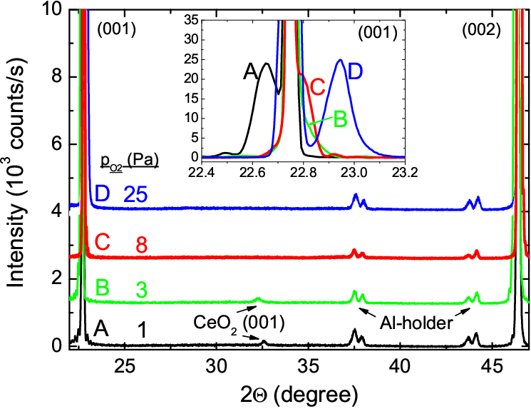
Figure 1 shows the XRD scans of four LCeMO thin films A, B, C, D (with similar thickness 90–100 nm) grown under different oxygen pressure 1, 3, 8 and 25 Pa, respectively. Sample C was in-situ annealed while the other samples were ”as-deposited“ films. According to the XRD data shown in Fig. 1, single phase LCeMO films were obtained for Pa (samples C and D). For a lower deposition pressure, impurity peaks of CeO2 appear (sample A and B). The substrate temperature also played a crucial role for the phase stability of the LCeMO films. By increasing up to C, CeO2 also appears for deposition pressures Pa. Such a behavior was also observed by Chang et al..[24] As shown in the inset of Fig. 1, the -axis decreases with increasing deposition pressure . This can be explained by a decreasing concentration of oxygen vacancies with increasing , as it is well known that oxygen vacancies tend to expand the lattice constants.[26]
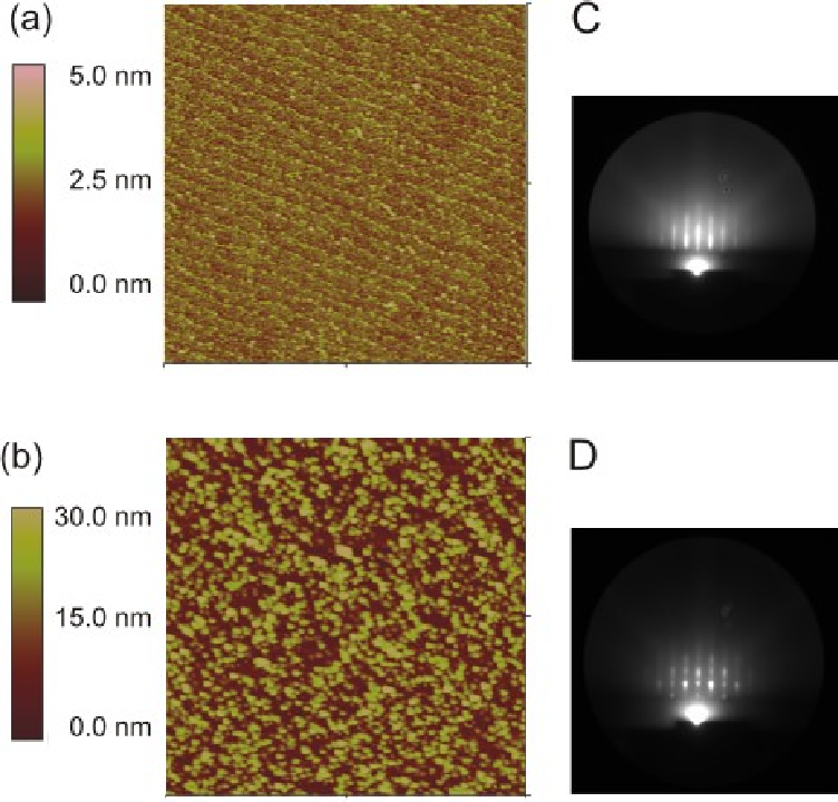
The surface roughness of the films depends strongly on deposition pressure, as shown by AFM and RHEED images on 100 nm thick films in Fig. 2 for (a) sample C (Pa) with an rms roughness of 0.35 nm and (b) sample D (Pa;), with a much larger rms value of 2.15 nm. The RHEED images show strong streaky patterns for the film deposited at Pa [Fig. 2(a) right], an indication of an atomically flat surface, while for higher deposition pressure [here Pa; Fig. 2(b) right] an increased surface roughness results in a combination of weaker streaks, together with the formation of a 3D RHEED pattern as a result of island growth. We note that sample C has an extremely smooth surface, showing unit-cell high terrace steps in the AFM image [c.f. Fig. 2(a) left], which is quite unusual for such a thick LCeMO film. A similar morphology as for sample C was observed for all films deposited at an oxygen pressure in the range of 1-8 Pa. For those conditions the films followed a 2D growth mode, as suggested by the RHEED and AFM data. Increasing the deposition pressure resulted in an increased step density during growth due to lower surface mobility, with the formation of 3D islands. Altogether, we found that Pa was the optimum pressure for growing films without measurable CeO2 concentration, as detected by XRD, and good surface morphology (rms roughness below 0.4 nm).
In order to evaluate the relation between CeO2 formation and the substrate induced strain, 50 nm thick LCeMO films were deposited on (001) STO, (110) NdGaO3 and (001) NdGaO3 substrates in the same deposition run.11 1 From the bulk values for the LCeMO lattice constants and [24] one obtains an in-plane lattice mismatch ranging from -2 % (tensile strain) to +1 % (compressive strain) for the different substrates used here. Here, we used a deposition pressure Pa, in order to obtain a measurable amount of CeO2. The XRD data showed no discernible difference in the amount of CeO2 for the different substrates.
The growth and phase stability of some complex oxide materials may depend on the type of termination layer of the substrate.[27] Therefore, we have grown several LCeMO films on (001) STO substrates with different termination (either SrO or TiO2) in order to determine whether the substrate termination influences the microstructure of the films. The SrO terminated substrates were obtained by annealing at C, for 1 h in an oxygen flow, while the TiO2-terminated STO substrates were obtained by chemical etching in a BHF solution, following the procedure described in Ref. [28]. The results showed no correlation between the substrate termination and the CeO2 impurity phase formation. These results suggest that, for the conditions used in this study, the level of strain and the type of substrate termination do not have an important effect on the phase stability in the LCeMO system and that, most probably, the deposition conditions (in particular and ) are the determining factors.
Figure 3 shows the evolution of the -axis with additional ex-situ annealing steps as obtained from XRD data for the (001) peak on sample E. As a result, the -axis decreased from Å to Å. As the - and -axis bulk values for LCeMO are smaller than the ones of the STO substrate, the observed shrinking of the -axis cannot be related to strain relaxation effects (which would increase ), but most probably to the incorporation of extra oxygen in the film. As another result of the annealing experiments, we did not find a correlation between ex-situ annealing and the CeO2 concentration in our films. This is in contrast to the observations presented by Yanagida et al.[21] and Chang et al.;[24] however, in their work, much longer annealing times (up to 10 hours) have been used. In our case, samples without secondary phase stayed single phase regarding the XRD data. However, while XRD data indicate that films deposited at 8-25 Pa O2 are single phase, HRTEM analysis showed evidence for phase separation even in these samples. The results of the microstructural TEM analysis are discussed in the following.

IV TEM
To obtain a better understanding on the relation between the microstructure and the physical properties of our LCeMO thin films, a few samples grown at different oxygen pressure were selected for TEM analysis. Here, we show results obtained from two films: sample E prepared at Pa, which appears single phase at XRD, and sample K prepared at Pa, containing CeO2 as secondary phase. TEM studies were carried out using a JEOL 4000EX microscope operated at 400 kV. The instrument has a point-to-point resolution of 0.17 nm. Planview TEM specimens were prepared by mechanical polishing of the samples down to a thickness of m, followed by Ar ion-milling at grazing incidence to reach electron transparency.
Figure 4(a) shows a HRTEM plan view image of the LCeMO thin film grown at 8 Pa O2 (sample E). Several CeO2 nanoclusters are indicated by arrows. A more detailed HRTEM image of one of the clusters is shown in Fig. 4(b). Figure 4(c) shows a TEM plan view image of the LCeMO thin film grown at 3 Pa O2 (sample K). In this sample, a higher density of CeO2 nanoclusters in comparison to sample E is observed. Furthermore, the size of the clusters is also larger (although still within the nanometer region). The interface between the CeO2 nanoclusters and the matrix is better defined in comparison to sample E.

HRTEM data for the analyzed samples prove the presence of CeO2 nanoclusters in the perovskite matrix (LCeMO) and show that CeO2 segregation in the 3 Pa sample is larger than in the 8 Pa sample. In case of the 8 Pa sample (and for another 25 Pa film not shown) the small total volume of CeO2 clusters made them untraceable by XRD. As an important consequence, our TEM data show that even LCeMO films which appear to be single phase from XRD data contain CeO2 nanoclusters. This observation is important, as it has been shown [21] that the valence state of Mn in LCeMO is sensitive to the degree of Ce segregation, which drives the valences from Mn3+ to Mn4+, even in the presence of Ce4+.
V Transport and magnetic properties

Figure 5 shows resistivity versus temperature for samples A, B and E. Sample A was ”as-deposited“ at Pa and shows no metal-to-insulator transition at all. Due to its high resistivity we could not trace out below K. Sample B, grown at 3 Pa (also ”as-deposited“) shows a slight indication of a metal-to-insulator transition, i. e. a maximum in at K, with a strong increase in resistivity at K, which can be explained by charge localization. Sample E, grown at 8 Pa (annealed in-situ) shows a transition at K.
For sample E, the evolution of the curves after two annealing steps (c. f. Sec.II) is additionally shown. The transition temperature increases to 230 K, which is accompanied by a decreasing resistivity, presumably due to an increasing charge carrier density. This observation is consistent with results obtained by Yanagida et al.[21] and contradicts the picture of an electron-doped manganite: Oxygen annealing should decrease the concentration of Mn2+ ions, hence, reduce the density of electrons as charge carriers and therefore lower and increase resistivity.[19] The annealing steps seem to create more Mn4+ in the samples, and the double-exchange between Mn3+ and Mn4+ gets stronger, which leads to an increase of . This interpretation is also supported by the results from measurements of the saturation magnetization () and the spectroscopic analysis, which will be discussed further below.
Figure 5 also shows that of sample B increases more drastically than sample E, even after only a single ex-situ annealing step. This might be due to the higher concentration of a secondary phase (CeO2) in sample B (c. f. Fig. 1), which may favor oxygen diffusion into the film due to crystal defects.

In Fig. 6 the magnetization (in units of Mn site) vs. applied field at K is shown for sample B, measured ”as grown“ (B1) and after ex-situ annealing (B2). The ex-situ annealing step caused a decrease in the saturation magnetization , from 2.93 to /Mn-site, while increased from 175 to 250 K. With the magnetic moments 5, 4 and for Mn2+, Mn3+ and Mn4+, respectively, the theoretical value for the saturation magnetization of electron-doped LCeMO is /Mn-site.[29] Until now, this value has never been achieved. However, for the hole-doped manganites, it is known that excess oxygen increases the valences from Mn3+ to Mn4+, and therefore decreases the magnetization. Hence, the observed decrease in with oxygen annealing can be explained by the decrease in Mn2+ and concomitant increase in Mn4+ concentration.

In order to study the dependence of structural, transport and magnetic properties on film thickness , four samples (C, E, F, G with =100, 65, 40 and 20 nm, respectively) were grown under the same conditions, i.e., at Pa with in-situ annealing. The XRD scans of the (001) peak in Fig. 7(a) show that with decreasing film thickness the -axis shrinks [see inset]. Assuming a fixed unit cell volume, this observation might be explained by increasing tensile strain with decreasing , as the bulk in-plane lattice parameters of LCeMO are smaller than those for the STO substrate. However, as oxygen vacancies tend to expand the lattice parameters, an increasing lack of oxygen with increasing has the same effect. The transport properties shown in Fig. 7(b) indicate exactly this lack of oxygen with increasing film thickness. Sample C, with largest , shows again charge localization at low , while the thinnest film has the highest [c. f. inset] and lowest . ¿From magnetization measurements on samples C, E, F and G we also find that increases with [c. f. inset in Fig. 7(b)]. The lowest saturation magnetization for the thinnest sample G is another indication for the higher oxygen concentration compared to the others.
VI Hall measurements
In order to determine the type of majority charge carriers via the Hall effect, we chose one of our films (sample H, nm) which was deposited at relatively low oxygen pressure (Pa) and cooled in 1 bar, without an annealing step. ¿From measurements of the longitudinal resistivity of the patterned film we find a clear MI transition with rather high K. The Hall resistivity was measured at , 50 and 100 K in magnetic fields up to 14 T. The sign of the Hall voltage was carefully checked by using an -doped silicon reference sample. Figure 8 shows vs. applied magnetic field . The drop of in the low-field range reflects the so-called anomalous Hall Effect, , which is due to spin orbit interaction.[30] Here, is the Hall coefficient for the anomalous Hall effect. With further increasing field, the data show the expected linear behavior of the normal Hall effect with Hall coefficient and charge carrier density . The main feature in Fig. 8 is the positive slope at high fields, which reveals the majority of the carriers to be holes with , 1.60 and , for , 50 and 100 K, respectively. This corresponds to 0.94–1.07 holes/Mn-site. The observation of hole-doping is consistent with the results from transport and magnetization measurements discussed above and also with the spectroscopic analysis, which will be presented in the following section.

VII Spectroscopic Analysis
X-ray Absorption Spectroscopy (XAS) was performed on LCeMO thin films prepared under different conditions, in order to investigate the relation between the manganese valences, the oxygen content and transport and magnetic properties. In total electron yield (TEY) detection mode only the uppermost 5 - 10 nm are probed, depending on the electron escape depth, while in fluorescence yield (FY) mode x-ray photons are detected. They have typical attenuation lengths from 100 nm (Ce M edge) to 200 nm (O K and Mn L edge), thus giving insight into the bulk structure of the samples.
Here we compare two films, D (as-deposited) and G (in-situ annealed), which were deposited at different oxygen pressure Pa and 8 Pa, respectively. ¿From XPS measurements we find that the oxygen content of G is higher than the one of D. This shows that the higher deposition pressure (for sample D) is not the key to higher oxygen concentration, but that annealing is most relevant. Sample G shows a MI transition at 232 K [c. f. Fig. 7(b)], while sample D shows a weak transition at 180 K and charge localization at lower temperatures.
A typical spectrum of the O K edge of LCeMO, measured in bulk sensitive fluorescence yield (FY) mode, is seen in Fig. 9 (left). The first structure at about 530 eV arises from transitions from the O1s level to states, which are commonly understood to be of mixed Mn3d-O2p character and as being a measure of the hole concentration.[31, 32, 33] In fact we found that this prepeak is stronger in sample G, i.e. the more oxidized sample. The second, rather broad and asymmetric feature at 532 to 537 eV is attributed to La5d (Ce), La4f (Ce) states hybridized with O2p states. A third set of states (not shown here) is found at about 543 eV and is widely believed to derive from hybridization of O2p with higher energy metal-states like Mn 4sp and La 6sp.[31]

The corresponding spectrum at the Mn L edge taken in TEY detection mode is shown in Fig. 9 (right). Both, the L3 edge at 642 eV and the L2 edge at 653 eV (not shown here) are strongly broadened, indicating the presence of a variety of valence states. The most important feature is the shoulder at 640 eV, which is a clear indication of divalent Mn, as can be shown by a comparison with XAS data from MnO.[34] In Fig. 9 (right) this shoulder is more pronounced in sample D, i.e., the less oxidized sample. The relative spectral weight of this feature in combination with the relative intensity of Mn3d-O2p states taken from the O K edge is essential to explain the properties of the different samples. A higher degree of oxidation leads to a higher relative spectral weight of the O K prepeak and a lower amount of Mn2+. By introducing more oxygen, more holes are created and the manganese valence is increased. This finding is further supported by measurements on three additional samples (not shown here), also showing the effect of film thickness, oxygen pressure during growth and duration of post-growth annealing in oxygen.
The remaining issue is the oxidation state of the Ce ions, which is important for the type of doping. Looking at the Ce absorption M5 edge both in surface-sensitive TEY detection mode and bulk-sensitive FY mode, we found striking differences in the spectral shapes of the measured spectra, as shown in Fig. 10(a). Cerium reference data for CeO2 and CeF3 were taken from Ref. [14]. In total electron yield detection mode the edge is identical to a pure CeO2 edge, i.e. cerium in a Ce4+ state. However, when increasing the information depth by switching to bulk sensitive FY detection,the edge changes drastically. The FY signal contains contributions from Ce4+ and Ce3+. Note that thermodynamically the reducing power of cerium is not sufficient for the Mn3+ - Mn2+ transition. The same trends are seen in the FY spectra of the Mn and O edges. Manganese reference data were taken from Ref. [35]. In case of the Mn edge [Fig. 10(b)] a decrease of the Mn2+ related feature at 640 eV is visible in the FY data, and the edges are broadened towards higher energies than in TEY mode. This indicates an increased amount of Mn3+ (642 eV) and Mn4+ (644 eV) species within the film as compared to the near surface region. Finally, at the O K edge (not shown here) the relative prepeak intensity at 530 eV increases with growing information depth from TEY to FY mode. As this feature is proportional to the hole concentration, this finding further emphasizes the point that the bulk is more oxidized than the surface and that the majority charge carriers are indeed holes.

VIII Conclusions
We investigated La0.7Ce0.3MnO3 thin films of variable thickness, grown epitaxially at different oxygen pressure and subjected to different oxygen annealing procedures. We find that thin film growth at low deposition pressure favors phase separation via the formation of CeO2 inclusions. For higher deposition pressure, still CeO2 nanoclusters are found, as shown by transmission electron microscopy, even for those films which appear to be single phase in x-ray diffraction analysis. Combining electric transport, magnetization and Hall measurements with x-ray photoemission and absorption spectroscopy we obtain a consistent picture in the sense that the appearance of a metal-to-insulator transition in electric transport measurements is always associated with hole doping and the presence of a mixed system of Mn2+, Mn3+ and Mn4+, despite finding Ce4+ as a sign of electron doping. The hole-doped behavior of our films may be explained by the presence of cation vacancies (due to CeO2 clustering), which can be occupied by excess oxygen that shifts the valences from Mn2+ to Mn3+ or Mn4+. In particular, oxidation states are well reproduced in the x-ray absorption spectra and fit to the transport properties. Upon oxidizing the samples, the system goes towards Mn3+ / Mn4+ as expected, while reducing the films forms more Mn2+ species. In particular for less oxidized films, we find a reduced layer at the surface with a more oxidized bulk underneath. This explains some of the peculiarities of this system, namely the discrepancy between finding Mn2+ and Ce4+ and still having holes as majority carriers. Furthermore, this demonstrates that one has to be very careful in relating surface sensitive spectroscopy data to bulk sensitive transport and magnetization data.
Acknowledgements.
We gratefully acknowledge Kathrin Dörr for helpful discussions and Matthias Althammer and Sebastian Gönnenwein for their support with the Hall measurements. Furthermore, we acknowledge the ANKA Angstroemquelle Karlsruhe for the provision of beamtime and we would like to thank P. Nagel, M. Merz and S. Schuppler for the skillful technical assistance using beamline WERA and for valuable discussions. This work was funded by the Deutsche Forschungsgemeinschaft (project no. KO 1303/8-1) and by the European Union under the Framework 6 program for an Integrated Infrastructure Initiative, ref. 026019 ESTEEM. S. B. thanks the Fund for Scientific Research – Flanders.References
- [1] M. Imada, A. Fujimori, and Y. Tokura, Rev. Mod. Phys. 70, 1039 (1998).
- [2] J. M. D. Coey, M. Viret, and S. von Molnar, Adv. Phys. 48, 167 (1999).
- [3] M. B. Salamon and M. Jaime, Rev. Mod. Phys. 73, 583 (2001).
- [4] A. J. Millis, Nature 392, 147 (1998).
- [5] A. J. Millis, P. B. Littlewood, and B. I. Shraiman, Phys. Rev. Lett. 74, 5144 (1995).
- [6] C. Zener, Phys. Rev. 81, 440 (1951).
- [7] P. W. Anderson and H. Hasegawa, Phys. Rev. 100, 675 (1955).
- [8] G. H. Jonker and J. H. Van Santen, Physica 16, 337 (1950).
- [9] P. Mandal and S. Das, Phys. Rev. B 56, 15073 (1997).
- [10] J. R. Gebhardt, S. Roy, and N. Ali, J. Appl. Phys. 85, 5390 (1999).
- [11] R. Ganguly, I. K. Gopalakrishnan, and J. V. Yakhmi, J. Phys.: Condens. Matter 12, L719 (2000).
- [12] Z. W. Li, A. H. Morrish, and J. Z. Jiang, Phys. Rev. B 60, 10284 (1999).
- [13] G. T. Tan, S. Dai, P. Duan, Y. L. Zhou, H. B. Lu, and Z. H. Chen, Phys. Rev. B 68, 014426 (2003).
- [14] C. Mitra, Z. Hu, P. Raychaudhuri, S. Wirth, S. I. Csiszar, H. H. Hsieh, H.-J. Lin, C. T. Chen, and L. H. Tjeng, Phys. Rev. B 67, 092404 (2003).
- [15] J. Philip and T. R. N. Kutty, J. Phys.: Condens. Matter 11, 8537 (1999).
- [16] C. Mitra, P. Raychaudhuri, G. Köbernik, K. Dörr, K.-H. Müller, and L. Schultz, Appl. Phys. Lett. 79, 2408 (2001a).
- [17] P. Raychaudhuri, S. Mukherjee, A. K. Nigam, J. John, U. D. Vaisnav, and R. Pinto, J. Appl. Phys. 86, 5718 (1999).
- [18] S. W. Han, J. D. Lee, K. H. Kim, C. Mitra, J. I. Jeong, K. J. Kim, B. S. Kim, B. I. Min, J. H. Kim, S. C. Wi, et al., Phys. stat. sol. 241, 1577 (2004).
- [19] D. J. Wang, J. R. Sun, S. Y. Zhang, G. J. Liu, B. G. Shen, H. F. Tian, and J. Q. Li, Phys. Rev. B 73, 144403 (2006).
- [20] Y. Zhao, R. Srivastava, P. Fournier, V. Smolyaninova, M. Rajeswari, T. Wu, Z. Li, R. Greene, and T. Venkatesan, J. Magn. Magn. Mater. 220, 161 (2000).
- [21] T. Yanagida, T. Kanki, B. Vilquin, H. Tanaka, and T. Kawai, Phys. Rev. B 70, 184437 (2004).
- [22] T. Yanagida, T. Kanki, and B. Vilquin, J. App. Phys. 97, 33905 (2005).
- [23] C. Mitra, P. Raychaudhuri, J. John, S. K. Dhar, A. K. Nigam, and R. Pinto, J. App. Phys. 89, 524 (2001b).
- [24] W. J. Chang, J. Y. J. C. C. Hsieh, K. H. Wu, T. M. Uen, Y. S. Gou, C. H. Hsu, and J.-Y. Lin, J. Appl. Phys. 96, 4357 (2004).
- [25] J. Töpfer and J. B. Goodenough, J. Solid State Chem. 130, 117 (1997).
- [26] P. Murugavel, J. H. Lee, J.-G. Yoon, T. W. Noh, J.-S. Chung, M. Heu, and S. Yoon, Appl. Phys. Lett. 82, 1908 (2003).
- [27] J. M. Huijbregtse, J. H. Rector, and B. Dam, Physica C 351, 183 (2001).
- [28] G. Koster, B. L. Kropman, G. J. H. M. Rijnders, D. H. A. Blank, and H. Rogalla, Appl. Phys. Lett. 73, 2920 (1998).
- [29] Q. Zhang and W. Zhang, Phys. Rev. B 68, 134449 (2003).
- [30] R. Karplus and J. M. Luttinger, Phys. Rev. 95, 1154 (1954).
- [31] M. Abbate, F. M. F. de Groot, J. C. Guggle, F. A, O. Strebel, F. Lopez, M. Domke, G. Kaindl, G. A. Sawatzky, M. Takano, et al., Phys. Rev. B 46, 4511 (1992).
- [32] N. Mannella, A. Rosenhahn, M. Watanabe, B. Sell, A. Nambu, S. Ritchey, E. Arenholz, A. Young, Y. Tomioka, and C. S. Fadley, Phys. Rev. B 71, 125117 (2005).
- [33] W. J. Chang, J. Y. Tsai, H.-T. Jeng, J.-Y. Lin, K. Y.-J. Zhang, H. L. Liu, J. M. Lee, J. M. Chen, K. H. Wu, T. M. Uen, et al., Phys. Rev. B 72, 132410 (2005).
- [34] M. Nagel, I. Biswas, P. Nagel, E. Pellegrin, S. Schuppler, H. Peisert, and T. Chassé, Phys. Rev. B 75, 195426 (2007).
- [35] B. Gilbert, B. H. Frazer, A. Belz, P. G. Conrad, K. H. Nealson, D. Haskel, J. C. Lang, G. Srajer, and G. D. Stasio, J. Phys. Chem. A 107, 2839 (2003).
- [36] L. Tröger, D. Arvanitis, K. Baberschke, H. Michaelis, U. Grimm, and E. Zschech, Phys. Rev. B 46, 3283 (1992).