Electronic Phase Separation Transition as the Origin of the
Superconductivity and the Pseudogap Phase of Cuprates
Abstract
We propose a new phase of matter, an electronic phase separation transition that starts near the upper pseudogap and segregates the holes into high and low density domains. The resulting grain boundary potential favors the development of intragrain superconducting amplitudes. The zero resistivity transition arises only when the intergrain Josephson coupling is of the order of the thermal energy and phase locking among the superconducting grains takes place. We show that this approach explains the pseudogap and superconducting phases in a natural way and reproduces some recent scanning tunneling microscopy data.
pacs
74.20.-z, 74.25.Dw, 74.72.Hs, 74.62.DhThe nature of the pseudogap phase has been widely recognized to be a key for understanding the physics of cuprate superconductors and its complex phase diagram[1, 2]. At present there is no consensus on its origin and also no agreement on the detailed generic doping dependence of the pseudogap temperature [2]. This difficulty to find an explanation for the data collected by many different experiments is certainly due to the intricate charge dynamics of cuprate superconductors.
To deal with this complicate charge dynamics we have proposed a static phase separation[3, 4, 5, 6] based on the experimental evidences of ion diffusion in and in Bi2212 above room temperature. The experimental signals that can be linked with a phase separation are observed at the upper pseudogap (in the notation of Ref.[1]) and consequently the ionic segregation transition must occur at a higher temperature . Since ( and ) falls to zero in the overdoped regime and ionic mobility requires high temperatures, we assumed previously a charge disorder for underdoped compounds and an uniform charge distribution for [5, 6, 7]. However, new scanning tunneling microscopy (STM) data have shown an inhomogeneous local gap structure that remains in the far overdoped regime[8, 9, 10] which cannot be explained by an ionic phase separation, due to the low values of for large .
These STM results on different doping regimes have clearly observed local gaps with different amplitudes at temperatures below and above [9, 10] that ruled out ionic phase separation as the sole origin of the cuprate inhomogeneities. In order to have an unified description of the STM data in the overdoped and underdoped regions of the phase diagram, we define a distinct phase of matter, an electronic phase separation (EPS). In this transition, the electrons (or holes) generate bubbles as the temperature decreases below the onset temperature and freezes at lower temperatures.
The origin of this novel EPS transition is the proximity to the insulator AF phase, common to all cuprates, and can be described in terms of competing minimum free energy or maximum entropy. As the temperature decreases, the entropy of the homogeneous density becomes lower than the anisotropic system made of a granular bimodal distribution[3] of AF domains with and high hole density domains with . This condition can be written as:
| (1) |
Where is the well known specific entropy of a homogeneous fermion gas with density , is the Onsager specific entropy for a 2D Ising model with spin coupling value that yields a Néel temperature at K, taken as a model to the AF phase[11]. is the entropy of mixing[12]. In Fig.(1) we show the condition for the EPS transition onset for some selected values of , when the straight lines cross the . The used value of is consistent with the entropy measurements[13]. The calculated are in general agreement with the upper pseudogap values[1, 2] and, more importantly, it provides a physical interpretation for the origin of the electronic inhomogeneities in the cuprates.

Now that we have discussed why cuprates may go through a transition to form granular charge domains, we need to describe quantitatively such transition. For this purpose we use the theory of Cahn-Hilliard (CH)[12] that is appropriate to describe a phase separation transition. The difference between the local and the average charge density is the order parameter. Clearly corresponds to a homogeneous system above . Then the typical Ginzburg-Landau free energy functional in terms of such order parameter near the transition is given by
| (2) |
Where the potential , , and are constants that lead to lines of constant values of , parallel to , as shown in the inset of Fig.(2). gives the size of the grain boundaries among two low and high density phases [14, 4]. The energy barrier between two grains of distinct phases is that is proportional to near the transition, and becomes nearly constant for temperatures close to . Thus, hereafter we will use as the grain boundary potential. and we assume, for simplicity, that have a linear behavior, whose equipotentials are parallel to . In the inset of Fig.(2) we plot , both assumed linear and the equipotentials are for .
For completeness, the CH equation can be written[15] in the form of a continuity equation of the local free energy , , with the current , where is the mobility or the charge transport coefficient. Therefore,
| (3) |
We have already made a detailed study of the density profile evolution in a array as function of the time steps, up to the stabilization of the local densities, for parameters that yield stripe[5] and patchwork[4, 16] patterns.
The temperature evolution of the second order EPS is studied by the ratio [16]. is close to the value of the measured upper pseudogap temperature shown in the inset of Fig.(2). At , the EPS domains are clearly formed as displayed in Fig.(2) and the system is on the limit between a disordered metal with grains of two densities, and a mixture of metallic and insulator (AF) grains. This is possibly the origin of the instability that falls to zero near p=0.18 as seen by may experiments[2, 13, 17] but not detected by the STM data for the Bi2212 series[8]. At K the domains are frozen and in general the low density insulator regions decrease in number and size as increases, but even overdoped samples have some remaining AF grains according to our simulations, what is also experimentally verified by the neutron diffraction data[18].

We study the free energy evolution with time and temperature together with the corresponding density profile. In Fig.(3) we show the free energy map associated with the density profile of Fig.(2), both made by the same computer simulation. It shows that the low and high density grains, at this temperature ( of for ), are already bound regions of free energy minimum.
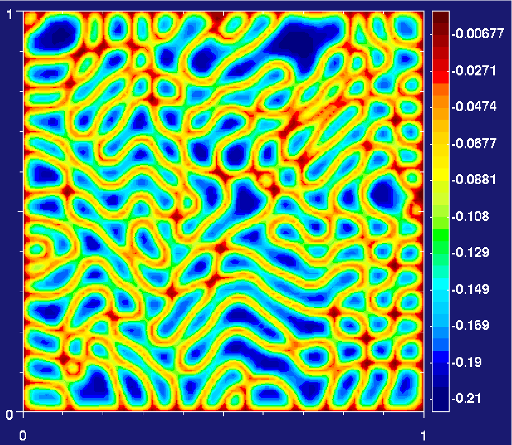
As the temperature decrease below , the potential barrier among the grains or the intragrain potential increases and becomes constant at low temperatures. Consequently the holes become confined by this effective attraction toward the center of the grains and it may be taken as the origin of the superconducting interaction that forms the (intragrain) hole pairs.
The intragrain superconductivity is naturally study with the Bogoliubov-deGennes (BdG) theory in a similar fashion as we did before for a phenomenological potential and a static phase separation[4, 5, 6]. The calculations are performed on a square lattice of sites, that is, on a small part of the charge density profile given in Fig.(2).
Assuming the extended Hubbard Hamiltonian to describe the hole dynamics, the diagonalization is made by the BdG equations[4, 5, 6, 16] with the hopping value eV, next neighbor hopping , on-site repulsion and, most importantly, the EPS next neighbor attraction derived from the values of . Except from the temperature dependent , all the others parameters are similar to values previously used[4, 5, 6].
Following our free energy simulations, from low temperatures up to when the grains melt down, we can obtain the qualitative behavior of . In order to yield average coherent gaps values comparable with to the STM data on Bi2212 compounds[8], we find a set of parameters that can be written as
| (4) | |||||
where the values are in , is linear and vanishes at following . falls to zero near and increases towards K.
In general, the CH and BdG combined calculations yield very low or almost zero local gaps for the regions with low densities, that is, . At the grains with larger local densities , the local Fermi level is large enough to have d-wave superconducting amplitudes . We define the local superconducting temperature as the temperature which arises in one given site ”i”. The largest value of in a given compound determines the pseudogap temperature which marks the onset of superconductivity. Since is close related with the potential it also increases in the overdoped region, similar to the Nernst effect[19] and many other experiments[1, 2].
As the temperature decreases below and some high density grains become superconductors, the zero resistivity transition takes place when the Josephson coupling among these grains is sufficiently large to overcome thermal fluctuations, that is, what leads to phase locking and long range phase coherence. Consequently the superconducting transition in cuprates occurs in two steps, similar to a superconducting material embedded in a non superconducting matrix[20], first by the appearing of intragrain superconductivity and by Josephson coupling with phase locking at a lower temperature, what provides a clear interpretation to the pseudogap phase. Since is not directly related with the local or intragrain superconductivity, the gaps do not change appreciably around , specially for underdoped compounds that have large . This fact is verified experimentally by temperature dependent tunneling[21] and angle resolved photon emission[22].
Using now the theory of granular superconductors[23], where is the normal conductivity among the grains. As shown in Fig.(2) the grain boundaries are made of walls with the mean density surrounding the grains. On the other hand, the conductivity increases a few orders of magnitude with in the plane[24] and is small in the underdoped region. That is just the opposite average behavior of that, following , decrease as increases. This gives some insights on the superconducting ”dome shape” of the resistivity transition with the maximum around in the middle of the EPS region (). Also , where is the critical current density and is the average size of the grains. Taking typical optimum doping values[25], that is, and as one can see directly from our Fig.(2), we get meV or K, which is a good estimate for the Bi2212 optimum .
Now we turn to the new STM data that motivated the introduction of the EPS concept. We firstly notice that the presence of the AF insulator () and even low density domains () which are closer to the half filled band and requires a high energy cost to accept extra electrons explains why injection of electrons produces less STM current than extraction and also why this asymmetry increases drastically as decreases[26].

Fig.(4) shows some of the local BdG calculations on selected points over a plane as in Fig.(2) to compare with the high temperature STM data of overdoped () Bi2212 compounds[9, 10]. The smaller coherent gaps are from different locations on metallic grains. The larger gaps originated in the insulator grains and are due to activation over the grain boundary barrier and the calculated from a metallic neighbor grain . As one can see in the experimental maps, at temperatures above , they are always surrounded by a small superconducting region[9, 10].
An interesting consequence of this scenario is that the lower density (insulator) grains have larger gaps but lower local conductivity that was verified experimentally[10]. Another consequence is that, despite the uncertainty on for very small gaps, the results follow close the measured relation [9].

In Fig.(5) we use our local gap calculation to plot the ratio between the tunneling conductance in the normal and in the superconducting state as measured by Pasupathy et al[10]. Our calculation is made with their Eq.(2). As mentioned above, for the case of insulator grains, the total gap is the grain boundary barrier plus the from a neighbor metallic grain. In Fig.(5) we used meV and =10mev similar to the larger gap of Fig.(4). Also, in the electronic granular scenario, due to the charge density oscillations and charge tunneling through the grains, the local inverse lifetime of the quasiparticle excitations[27] is an oscillating function of the applied bias and the temperature. As shown in Fig.(5) this phenomenological form of yields the measured density of states[10] with a structure near the applied voltage eV that is captured by our calculations.
In conclusion we have proposed a new electronic phase to cuprate superconductors essentially made of disordered low and high charge density grains. The grains are static at low temperatures but melts slowly and disappear near . Such anomalous phase arises due to the proximity of the undoped insulator with AF order, and may be common to other materials with some doping dependent phases, like manganites which possess also a pseudogap phase[28].
We gratefully acknowledge partial financial aid from Brazilian agency CNPq.
References
- [1] T. Timusk and B. Statt, Rep. Prog. Phys., 62, 61 (1999).
- [2] J.L. Tallon and J.W. Loram, Physica C 349, 53 (2001).
- [3] E.V.L. de Mello et al, Phys. Rev. B67, 024502 (2003).
- [4] E.V.L. de Mello, and E.S. Caixeiro, Phys. Rev. B70, 224517 (2004).
- [5] E. V. L. de Mello, and D. N. Dias, J. Phys. C.M. 19, 086218 (2007).
- [6] D. N. Dias et al, Phys. C 468, 480 (2008).
- [7] D. N. Dias et al, Phys. Rev. B76, 90737 (2007).
- [8] K. McElroy, et al cond-mat/0404005 an Phys. Rev. Lett. 94, 197005 (2005).
- [9] Kenjiro K. Gomes et al, Nature 447, 569 (2007).
- [10] Abhay N. Pasupathy et al, Science 320, 196 (2008).
- [11] H. E. Stanley, ”Introductin to Phase Transitions and Critical Phenomena” (Oxford U. Press, N.Y., 1971).
- [12] J.W. Cahn and J.E. Hilliard, J. Chem. Phys, 28, 258 (1958).
- [13] J.W. Loram et al, J. Phys. Chem. Sol. 62, 59 (2001).
- [14] E.V.L de Mello, and Otton T. Silveira Filho Physica A 347, 429 (2005).
- [15] A.J. Bray, Adv. Phys. 43, 347 (1994).
- [16] E.V.L. de Mello et al, Proceedings of SCES08, submitted to Physica B (2008).
- [17] J. E. Sonier et al , Phs. Rev. Lett. 101, 117001 (2008).
- [18] S. Wakimoto et al, Phys. Rev. Lett. 98, 247003 (2003).
- [19] Yayu Wang, Lu Li, and N. P. Ong, Phys. Rev. B 73, 024510 (2006).
- [20] L. Merchant et al, Phys. Rev. B63, 134508 (2001).
- [21] Minoru Suzuki, and Takao Watanbe, Phys. Rev. Lett., 85, 4787 (2000).
- [22] A.Kanigel et al, Phys. Rev. Lett. 101, 137002 (2008).
- [23] V. Ambeogakar, and A. Baratoff, Phys. Rev. Lett. 10, 486 (1963).
- [24] H. Takagi et al, Phys. Rev. Lett. 69, 2975 (1992).
- [25] J. L. Tallon et al, Phys. Stat. Sol 215, 531 (1999).
- [26] Y. Kohsaka et al, Science 315, 1380 (2007).
- [27] R. C. Dynes, V. Narayanamurti, and J. P. Garno, Phys. Rev. Lett. 41, 1509 (1978).
- [28] E. Dagotto et al, Sol. Stat. Comm. 126, 9 (2003).