Out-of-equilibrium singlet-triplet Kondo effect in a single quantum dot
Abstract
We have used an electromigration technique to fabricate a single-molecule transistor (SMT). Besides describing our electromigration procedure, we focus and present an experimental study of a single molecule quantum dot containing an even number of electrons, revealing, for two different samples, a clear out-of-equilibrium Kondo effect. Low temperature magneto-transport studies are provided, which demonstrates a Zeeman splitting of the finite bias anomaly.
I Introduction
Single-molecule transistor (SMT) is the ultimate limit in miniaturizating three terminal electronic devices, consisting in two reservoirs (Source and Drain) and a gate (see Fig. 1a). While various experimental schemes have been proposed to address a single molecule quantum dot, one of the most attractive technique to realize a single-molecule transistor is the use of electromigration. This technique allows to realize nanometric gaps between electrodes by applying a controlled voltage ramp through a continuous metallic small wire. Due to the momentum transfer from the conduction electrons, and with some thermal enhancement due to Joule heating, metallic ions migrate and a nanogap between two electrodes is produced. If a single molecule is trapped during the electromigration process, due to nanometric confinement of the wave-function of the electrons in a SMT, Coulomb blockade phenomena are expected [1, 2, 3, 4, 5, 6]. Depending on the bias voltage and the gate voltage , the transistor can be tuned to allow current flowing or not through the single-molecule, resulting in Coulomb diamond diagrams (Fig. 3a). The number of observed Coulomb diamonds in a given gate voltage regime strongly depends on the gate depending coupling of to surroundings and on the charging energy of the SMT.
In the presence of an odd number of electrons in a SMT, when a spin-1/2 magnetic state of the quantum dot is strongly coupled antiferromagnetically to the electrons in the reservoirs, the electronic states of the quantum dot hybridise with the electronic states of the reservoirs. As a result, even if the energy of the quantum dot state is far below the Fermi level of the reservoirs, hybridisation creates an effective density of states on the site of the dot, which is pinned at the Fermi level of the reservoirs, leading to a zero-bias anomaly where a Coulomb gap would have naively been expected. This is known as Kondo effect in quantum dot devices [7, 8], and this signature has been widely observed in semiconducting devices [9, 10], carbon nanotube [11], or single-molecule [4, 12, 13] quantum dots. Universality is a fundamental property of the Kondo effect and a single energy scale, associated with the Kondo temperature , fully describes the physical properties at low energy. When the typical energy of a perturbation, such as temperature, bias voltage, or magnetic field, is higher than , the coherence of the system is suppressed and the Kondo effect disappears. However, a fundamental question is what happens when the quantum dot is occupied with an even number of electrons ? For a quantum dot with two electrons and two nearly degenerate orbital levels, two different kinds of magnetic states occur: a singlet and a triplet. We present then an experimental study of a single-molecule quantum dot with an even number of electrons and a singlet ground state. This SMT is strongly coupled to the electrodes, leading to an out-of-equilibrium singlet-triplet Kondo effect that we observed with two different based SMT. First, we present the set-up we have developed to realize the electromigration procedure and the measurements, then we explain how the SMT is prepared, and finally, we present our measurements.

II Set-up description and electromigration procedure
To our knowledge, no electromigration procedure has been previously carried out in a dilution refrigerator with a high degree of filtering of the electrical leads. Indeed, the creation of nanogaps with this technique requires minimizing the series resistance [14], which is generally incompatible with dilution fridge wiring and filtering. To overcome this problem, we developed a specific measurement setup (Fig. 2), which is divided into two parts, described here.
First, electromigration [15] is performed at 4 K with the fast part of the setup. As we wanted to perform such measurements in a dilution fridge, we developed an efficient electromigration technique since dilution wires and low-temperature filters are very resistive and add an important series resistance to the sample (few hundreds Ohms). Improvements of the original procedure [15] have already been reported recently [16, 17, 18, 19, 20, 21]. We ramp the voltage (typical rate is mV/s) across the gold nano-wire fabricated by shadow evaporation on an back gate (Fig. 1b), and measure its conductance using a very fast feedback-loop ( ). As shown on Fig. 1c, the procedure can be divided into three parts. First, we measure a decrease of the conductance due to Joule heating of the nanowire. In a second part, the conductance increases, due to the melting of part of the nanowire. Finally, when the voltage becomes too high, namely when the gold ions migrate, the conductance suddenly drops to much lower values, quantized in , as shown on Fig. 1d. Using the fast feedback-loop, we set the voltage to zero when the resistance exceeds a defined threshold, typically 20 k. The fast feed-back loop was achieved with real-time electronics (Adwin Pro II) and a home-built high-bandwidth current to voltage converter, as described in Fig. 2. With this technique, we obtained small gaps (Fig. 1b) characterized by the tunnel current measured after electromigration, without molecules, in previous experiments, resulting in a gap of the order of 1-2 nm.
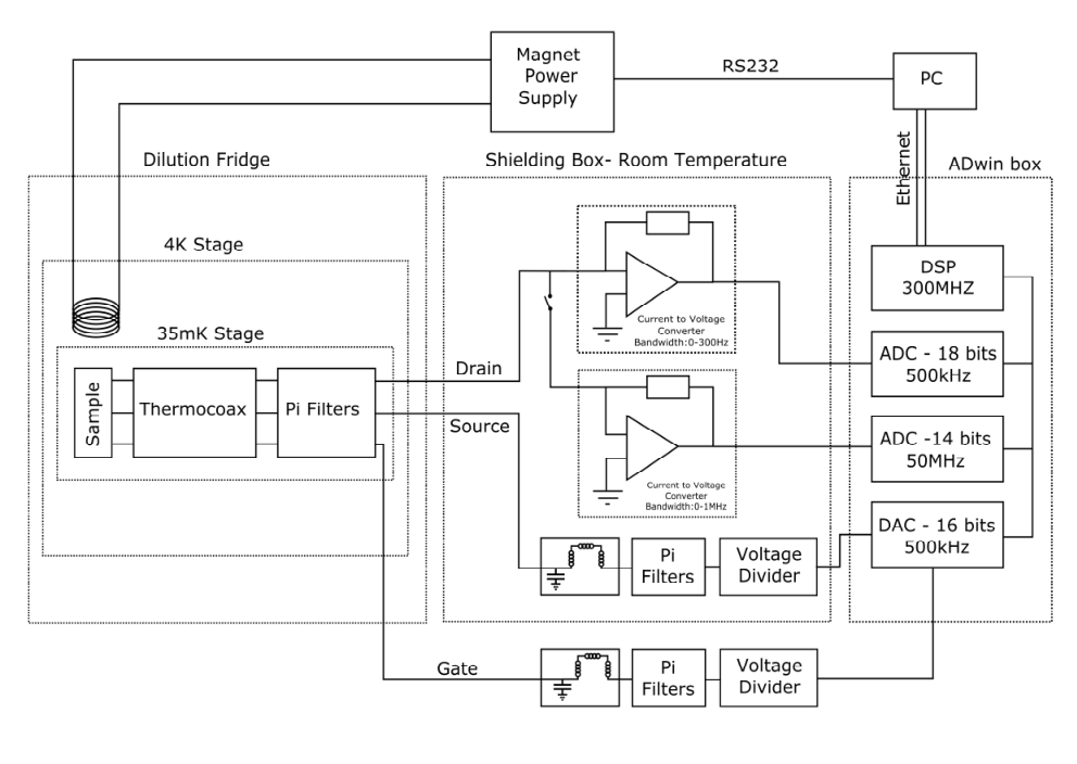
The second step uses the low noise component of the setup to measure the single-molecule transistor. In addition to low-temperature filtering, we used filters and ferrite bead filters developed at Harvard by J. MacArthur and B. D’Urso [22]. In order to minimise ground loops we integrated all the analogical electronics in a shielded box at room temperature. Because of its great versatility, Adwin Pro II can be programmed to perform DC or lock-in measurements, and apply gate or bias voltages, thus minimizing the possibility of ground loops. Depending on the measurements, we used an AC-excitation between 3 and 100 for the lock-in technique.
III Preparation of the single-molecule transistor
Preparation of the SMT was realized by blow drying a dilute toluene solution of a molecule onto a gold nanowire realized on an back gate, see Fig. 1a for a schematic view of the setup. Before blow drying the solution, the electrodes were cleaned with acetone, ethanol, isopropanol and oxygen plasma. The connected sample is inserted in a copper shielded box, enclosed in a high frequency low-temperature filter, anchored to the mixing chamber of the dilution fridge having a base temperature equals to mK. The nanowire coated with molecules is then broken by electromigration [15], via a voltage ramp at K. As it is known that even if the electromigration procedure is well controlled, there is always a possibility to fabricate a few atoms gold aggregate [17] transistor, we studied several junctions prepared within the same procedure with a toluene solution only. In our opinion, it is relevant to state here that an ”interesting” device to investigate must show at least one order of magnitude change in the current characteristics as a function of the gate voltage for a mV voltage bias, and a charging energy greater than meV. Within these restrictions, we tested bared junction with a toluene solution and with a dilute toluene solution. While bared junction showed one order of magnitude changes in the current as a function of the gate voltage after electromigration, only had a charging energy higher than meV, and only of those exhibited a zero bias anomaly. These transport structures were also not very well defined. For junctions prepared with a diluted toluene solution, we measured junctions out of with one order of magnitude changes in the current as a function of gate voltage, and of those had a charging energy higher than meV and exhibited pronounced zero bias anomalies. Here we report on an experimental study of transport measurements in a single-molecule QD, as a function of bias voltage , gate voltage , temperature ( mK K), and magnetic field up to T on two different samples labelled and .
IV Out-of-equilibrium singlet-triplet Kondo effect

In this section, we demonstrate, in our molecular junction, an effect recently reported by Paaske et al. in a carbon nanotube quantum dot [23], namely the out-of-equilibrium singlet-triplet Kondo effect. These authors were the first to clearly identify sharp finite features as a Kondo effect and not as simple cotunneling via excited states. The main idea behind Kondo physics is the existence of a degeneracy, which is lifted by the conduction electrons. This is clearly the case for a quantum dot with only one electron on the last orbital, leading to a doubly degenerate spin .
For a quantum dot with two electrons and two nearly degenerate orbital levels, two different kinds of magnetic states occur: a singlet and a triplet. Depending on , the energy difference between the two orbital levels, and , the strength of the ferromagnetic coupling between the two electrons, the splitting between the triplet and the singlet can in principle be tuned, and eventually brought to zero, leading to the so-called singlet-triplet Kondo effect [24]. However the singlet is in most situations the ground state, leaving the triplet in an excited state, thus suppressing the Kondo effect. Kondo signatures can nevertheless be observed by tuning the degeneracy in a magnetic field [11, 25, 26].
Another way to retrieve the degeneracy is to apply a bias voltage , although it is of course more delicate to preserve the quantum coherence necessary to Kondo correlations. Indeed, finite-bias features clearly linked to magnetic excitations were observed in 2DEGs [27], carbon nanotubes [11, 26, 28, 29] and even recently in an OPV5 molecule [30]. However, only the study reported by Paaske et al. [23] was able to identify a clear out-of-equilibrium Kondo effect. Their first observation was the occurence of sharp peaks in the differential conductance for both positive and negative bias voltage, very different from the cusps usually associated to cotunneling. Secondly the height of these peaks decreased logarithmically with temperature, which is another typical signature of Kondo correlations. Finally the shape of the peaks could be well accounted for in an out-of-equilibrium Kondo calculation, while a simple cotunneling model failed to reproduce the data.

These striking features are also present in our experiment, for the case of an even number of electrons into the single molecule for two different devices labelled sample A and sample B. These two-electron states can be described by their total spin and spin projection and are noted . The ground state of the system can thus be either a spin singlet with energy , or a spin triplet with energy described by the three states , degenerated at zero magnetic field, but split by the Zeeman effect, with an energy shift for each state , where for a molecule.
Beginning with sample A, we present in Fig. 3a a colour-scale map over two Coulomb diamonds of the differential conductance as a function of bias voltage and gate voltage at mK and zero magnetic field. Focusing in the right diamond with an even number of electrons, we present in Fig. 3b a precise low-bias map corresponding to the white rectangle in Fig. 3a. In this region, we define, in anticipation of our results, the singlet as the ground state of the quantum dot. A gate-dependent finite-bias conductance anomaly appears when coincides with , which is due to an out-of-equilibrium Kondo effect involving excitations into the spin-degenerate triplet. The possibility of gate-tuning the singlet-triplet splitting has already been demonstrated for lateral quantum dots [31], carbon nanotubes [29] and recently in SMT [13], and may originate from an asymmetric coupling of the molecular levels to the electrodes [32]. From now on we focus on the region where the singlet is the ground state, and present magneto-transport measurements to precisely identify these spin states.
Due to the high factor of a molecule, as compared for instance to in GaAs-based devices, it is easier to lift the degeneracy of the triplet state via the Zeeman effect. Fig. 3d investigates the gate-induced out-of-equilibrium singlet-triplet Kondo effect at a constant magnetic field of 8 T. As the singlet is the ground state, the Zeeman split triplet states are clearly measured as three parallel lines, which is in agreement with the energy levels depicted in Fig. 3c.
We now focus on sample B and present first a colour-scale map over one Coulomb diamond, corresponding to a region with an even number of electrons, of the differential conductance in Fig. 4a. At a fixed gate value , corresponding to the white line in a Fig. 4a, we present a measurement as a function of the magnetic field up to T in Fig. 4b. The splitting of the threefold triplet is, as for sample A, clearly observed. This plot, which was not numerically treated, shows the Zeeman splitting between the three triplet states at both positive and negative bias. The positions of those peaks are reported on Fig. 4b and a linear fit is applied to each line, with a very good accuracy which enables us to determine, firstly, a critical field of 50 mT before the splitting occurs, and secondly, a Lande factor . The existence of a critical field for the splitting of the zero-bias anomaly is well-documented in the case of the Kondo effect in equilibrium [33], while more theoretical work is needed in order to interpret this data [23].
In Fig. 4c, we present a measurement as a function of the voltage bias , for a constant gate voltage , for different temperatures. While the conductance at low bias is suppressed when the spin state of the system is a singlet, a clear finite-bias peak grows by decreasing temperature as shown in Fig. 4c. In addition, the amplitude of the positive bias peak decreases logarithmically about a decade (Fig. 4d), showing a clear signature of the out-of-equilibrium singlet-triplet Kondo effect.
To conclude, we have presented conductance, magneto-transport and temperature measurements on two different samples using an electromigration technique to realize a based single-molecule quantum dot. These two SMTs clearly exhibit out-of-equilibrium singlet-triplet Kondo effect when the ground state of the quantum dot is defined by the singlet. In our opinion, it is extremely interesting, despite challenging, to study SMT because the charging energy of a molecule is possibly much larger than that of a carbon nanotube quantum dot for example. Such systems allow to study new Kondo phenomena, such as quantum phase transition [13], at relatively high temperatures.
We gratefully acknowledge E. Eyraud, D. Lepoittevin for their useful electronic and dilution technical contributions and motivating discussions. We thank E. Bonet, T. Crozes and T. Fournier for lithography development, C. Winkelmann, M. Deshmukh, T. Costi and L. Calvet for invaluable discussions. The sample of the investigations was fabricated in the NANOFAB facility of the Institut Néel. This work is partially financed by ANR-PNANO Contract MolSpintronics.
References
- [1] H. Park et al.. Nature 407, 57 (2000).
- [2] J. Park et al.. Nature 417, 722-725 (2002).
- [3] D. R. Ward, G. D. Scott, Z. K. Keane, N. J. Halas & D. Natelson. J. Phys: Condens. Matter, 20, 374118 (2008).
- [4] W. Liang, M. P. Shores, M. Bockrath, J. R. Long & H. Park. Nature 417, 725-729 (2002).
- [5] S. Kubatkin et al.. Nature 425, 698-701 (2003).
- [6] A. R. Champagne, A. N. Pasupathy & D. C. Ralph. Nano Lett. 5, 305-308 (2005).
- [7] L.I. Glazman & M. E. Raikh. JETP letters 47, 452 (1988).
- [8] T. K. Ng & P. A. Lee. Phys. Rev. Lett. 61, 1768-1771 (1988).
- [9] D. Goldhaber-Gordon et al.. Nature 391, 156-159 (1998).
- [10] S. M. Cronenwett, T. H. Oosterkamp & L. P. Kouwenhoven. Science 281, 540-544 (1998).
- [11] J. Nygård, D. H. Cobden & P. E. Lindelof. Nature 408, 342-346 (2000).
- [12] L. H. Yu & D. Natelson. Nano Lett. 4, 79-83 (2004).
- [13] N. Roch, S. Florens, V. Bouchiat, W. Wernsdorfer & F. Balestro. Nature, 453, 633 (2008).
- [14] H. S. J. van der Zant et al. Faraday Discuss. 131, 347 (2006).
- [15] H. Park, A. K. L. Lim, A. P. Alivisatos, J. Park & P. L. McEuen. Appl. Phys. Lett. 75, 301-303 (1999).
- [16] D. R. Strachan et al. Appl. Phys. Lett. 86, 043109 (2005).
- [17] A. A. Houck, J. Labaziewicz, E. K. Chan, J. A. Folk & I. L. Chuang. Nano Lett. 5, 1685-1688 (2005).
- [18] G. Esen & M. S. Fuhrer. Appl. Phys. Lett. 87, 263101 (2005).
- [19] M. L. Trouwborst, S. J. van der Molen & B. J. van Wees. J. Appl. Phys. bf 99, 114316 (2006).
- [20] K. O’Neill, E. A. Osorio & H. S. J. van der Zant. Appl. Phys. Lett. bf 90, 133109 (2007).
- [21] Z. M. Wu et al. Appl. Phys. Lett. 91, 053118 (2007).
- [22]
The recipe of such filters can be found on C. Marcus website.
http://marcuslab.harvard.edu/how_to/Ferrite_Bead_Filter.pdf
- [23] J. Paaske et al. Nature Physics 2, 460-464 (2006).
- [24] J. Schmid, J. Weis, K. Eberl & K. v. Klitzing. Phys. Rev. Lett. 84, 5824-5827 (2000).
- [25] S. Sasaki et al. Nature 405, 764-767 (2000).
- [26] W. Liang, M. Bockrath & H. Park. Phys. Rev. Lett. 88, 126801 (2002).
- [27] D. M. Zumbühl, C. M. Marcus, M. P. Hanson & A. C. Glossard. Phys. Rev. Lett. 93, 256801 (2004).
- [28] B. Babić, T. Kontos & C. Schönenberger. Phys. Rev. B 70, 235419 (2004).
- [29] C. H. L. Quay et al. Phys. Rev. B, 76, 245311 (2007).
- [30] E. A. Osorio et al. Nano Lett. 7, 3336-3342 (2003).
- [31] A. Kogan, G. Granger, M. A. Kastner, D. Goldhaber-Gordon & H. Shtrikman. Phys. Rev. B 67, 113309 (2003).
- [32] J. V. Holm et al. Phys. Rev. B 77, 161406 (2008).
- [33] T. A. Costi. Phys. Rev. Lett. 85, 1504-1507 (2000).