Superconductivity-Enhanced Bias Spectroscopy in Carbon Nanotube Quantum Dots
Abstract
We study low-temperature transport through carbon nanotube quantum dots in the Coulomb blockade regime coupled to niobium-based superconducting leads. We observe pronounced conductance peaks at finite source-drain bias, which we ascribe to elastic and inelastic cotunneling processes enhanced by the coherence peaks in the density of states (DOS) of the superconducting leads. The inelastic cotunneling thresholds display a marked dependence on gate voltage caused by different tunneling-renormalizations of the two subbands in the nanotube. Finally, we discuss the gate-dependent sub-gap structure observed in a strongly coupled device with odd electron occupation.
pacs
73.21.La, 73.23.Hk, 73.63.Fg, 74.50.+rSuperconducting electrodes provide a useful means of sharpening the spectroscopic features observed in tunneling experiments. In the superconducting phase, an otherwise nearly constant DOS acquires a gap of width centered at the Fermi level and characteristic sharp coherence peaks at the gap-edges . These peaks transform a featureless metallic electrode into a high-resolution tunneling probe. This widely used investigative tool [1] was demonstrated already by Giaever’s seminal work [2] from 1960 and more recently used to obtain a high resolution bias-spectrum of the levels in a metallic Al-nanoparticle [3]. Here we report low-temperature transport measurements in which this type of BCS-focusing promotes an otherwise featuresless elastic cotunneling conductance to sharp peaks at bias voltages , corresponding to the onset of quasiparticle cotunneling. In the same way, inelastic cotunneling processes involving transitions between two subbands in the nanotube are revealed as sharp peaks rather than steps or cusps in the nonlinear conductance. This sharpening of cotunneling lines inside the Coulomb diamonds allows us to investigate more closely the tunneling-induced gate voltage dependence of the orbital splitting [4]. Finally, we discuss an unusual sub-gap structure observed in a particularly well coupled device, signalling the importance of both multiple Andreev reflections (MAR) and dynamically generated bound states in spinful dots. A number of experiments have already investigated interesting aspects of quantum dots with superconducting electrodes, such as supercurrent [5, 6, 7], MAR [8], and effects of size and charge quantization in the Fabry-Perot [9, 10, 11, 12], Kondo [13, 14, 15, 16, 17, 18], and Coulomb blockade regimes [19, 14, 20, 21, 22]. We present measurements performed on two different single walled carbon nanotube (SWCNT) quantum dots coupled to niobium-based superconducting leads [8, 7]. Our first device (device A) is poorly coupled to the leads and shows regular Coulomb blockade diamonds with clear onset of quasiparticle (elastic cotunneling) current. The second device (device B) is more strongly coupled to the leads and displays a four-fold degenerate shell structure with both elastic and inelastic cotunneling lines which are sharpened by the superconducting leads.

The devices are made by growing high quality SWCNT by chemical vapor deposition from predefined catalyst islands [10, 15]. Contacts are made of Nb-based trilayers, /Nb/ (about 5/60/10 nm), with =Pd,Ti where is thermally evaporated and the Nb is deposited by sputtering technique. The superconducting trilayers are tested via four terminal devices on the same chip and show transition temperatures close to K. Nevertheless, the actual gap at the nanotube indicates a critical temperature of K, which might be related to the formation of NbO ( K) [23] or contamination of the lower Nb/x interface. Samples from three different processing rounds revealed similarly reduced in transport measurements. However, the high quality of the presented measurements is a promising first step towards Nb based SWCNT Josephson junctions. Figure 1(a) shows the conductance versus gate, and bias voltage (bias spectroscopy plot) at K for device A consisting of a carbon nanotube quantum dot coupled weakly to Ti/Nb/Ti leads. It reveals more than 80 regular Coulomb diamonds, illustrating that only one quantum dot is defined in this high quality carbon nanotube. The charging energy, meV is estimated from the height of the diamonds and no clear shell structure is observed11 1 A variation of the addition energies is seen, but no clear four-electron shell structure is observed as is the case of device B. The origin of this difference is not understood, except that the energy scales related to device B are much larger than in device A, making such effects more visible.. A region of highly suppressed conductance around zero bias is clearly observed for all gate voltages reflecting the superconducting energy gap of the leads. Figure 1(b) shows the Coulomb diamonds in the dashed rectangle of Fig. 1(a). In Coulomb blockade (inside the diamonds) the onset of quasiparticle tunneling is seen as horizontal lines (conductance ridges) at meV (green arrows). Higher order Andreev reflections, which would lead to current below the gap, are strongly suppressed due to the poor coupling to the leads. Inside the diamonds, the onset of quasiparticle cotunneling corresponds to an alignment of the superconducting DOS peaks and involves elastic cotunneling processes as depicted in Fig. 1(c). At the charge degeneracy points, conductance inside the gap is due to Andreev reflections [19]. Figure 1(d) shows a bias cut slightly off resonance (I) and further off resonance (II). The onset of quasiparticle tunneling at (I) involves a sequential tunneling process and is therefore much stronger than in (II). Peaks at higher bias are due to sequential tunneling to ground and excited states, respectively.
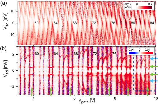
Figure 2(a) shows a bias spectroscopy plot for the second, better coupled, device (device B) at K well above the transition temperature ( K) of the superconducting Pd/Nb/Pd layer. A regular pattern is seen with three consecutive small Coulomb diamonds followed by a larger diamond, reflecting the filling of shells consisting of two nearly degenerate orbitals. Numbers in Fig. 2 denote the additional electron number on the SWCNT for filled shells counted from V. A charging energy of meV and a level spacing of meV are found from the plot. Figure 2(b) shows the conductance at K, i.e. below . The lines at mV (green horizontal arrows) are caused by elastic quasiparticle cotunneling as illustrated by Fig. 1(c). Inelastic cotunneling lines [Fig. 2(b), blue arrows] are observed at higher for electron numbers , , , but not in the full shell ( electrons). These lines have a marked gate voltage dependence which resembles the ’double-headed arrow’ structure pointed out in Ref. 4. With the enhanced spectroscopy offered by the superconducting leads we also observe an additional third ’arrowhead’ outside the strong elastic cotunneling lines appearing in every fourth (N+3) diamond, i.e. a possible Kondo ridge at this temperature in the normal state. The high and critical field of the Nb-films prevented us from confirming the presence of a normal-state Kondo resonance, insofar as this resonance would already be suppressed by the magnetic field. The inelastic cotunneling lines are seen more clearly in Fig. 3(a) which shows detailed measurements from the dashed rectangle in Fig. 2(b). The cotunneling processes are depicted in Fig. 3(b-e), involving a weaker coupled orbital (orbital 1) [thin red line in Fig. 3(b)] and a stronger coupled orbital (orbital 2) [thick blue line in Fig. 3(b)] split by . Such processes are allowed for all but the charge state corresponding to a filled shell [Fig. 3(e)], consistent with Fig. 3(a). As demonstrated by Holm et al. [4], a difference in tunnel-couplings to the two orbitals in the quantum dot, gives rise to a gate-dependence of the threshold for inelastic cotunneling. With superconducting leads, such tunneling renormalization produces a gate-dependent shift of the unrenormalized threshold at , as observed.

In Fig. 4(a) we show conductance line-cuts through the center of each diamond 81-84 in Fig. 3(a). The variation of the peak heights can be understood from the number of elastic (EL) and inelastic (INEL) cotunneling channels in each diamond, as summarized in Table 1.
| Shell filling | 1 | 2 | 3 | 4 |
|---|---|---|---|---|
| EL | ||||
| INEL | 2 | 4 | 2 | 0 |
There, the EL notation indicates whether the tunneling takes place through the higher- or lower-energy orbital. For example, in case of filling 1 [see Fig. 3(b)], a total of 6 EL channels contribute: 2 from the upper and 4 from the lower orbital.
In Fig. 4(b) we show the results of a calculation of the lowest order nonlinear cotunneling conductance for the four different charge states in a single shell. The calculation involves the quasiparticle tunneling rates between leads and orbitals . For example, the rate for the process shown in Fig. 3(b) is
| (1) |
with the Fermi function, , and in terms of the tunneling amplitudes . Solving the steady-state rate equations we obtain the orbital occupation numbers as a function of and the current is readily determined. In agreement with experiment one sees from Fig. 4 that the inelastic cotunneling peak is largest for diamond 82 due to the larger number of tunneling possibilities. Likewise the elastic -peak is largest for diamond 83 due to the larger coupling of orbital 2 to the leads. The calculation does not reproduce the small shifts of some of the peaks seen in the experimental data, as well as the ratio between the amplitude of the elastic and inelastic peaks in diamond 81. We speculate that the latter discrepancy will be removed by including higher order processes involving the strongly coupled orbital 2. The width of the peaks arise from a small smearing factor () used in the DOS of the superconducting leads mimicking a constant inelastic scattering rate in the contacts. We ascribe the larger width of the measured peaks to tunnel-broadening of the excited states which is not included in the calculation.
For the results shown in Fig. 4 we have used meV, meV, meV, and meV, yielding an asymmetry factor in the order of consistent with an upper bound22 2 The Coulomb peaks measured at K are already slightly suppressed by temperature. of approximately 40 extracted from the Coulomb peak heights in the shell at 6.5K. The couplings are estimated from the sequential current at large positive () and negative bias () at the charge degeneracy point for adding the first electron in a four-fold degenerate shell. These currents are given by nA/ nA in reasonable agreement with the experiment at the Coulomb resonance involving electron charge states 80 and 81, nA/ nA. Moreover, the chosen couplings lead to a gate-voltage slope [4] of the inelastic line of (average meV), which agrees with the experimental result of [average slope of the cotunneling lines in diamonds 81-83 in Fig. 3(a)]. We note that since , the expression for the renormalization obtained in the normal state [4] remains valid in the case of superconducting leads. Based on the couplings used above, we estimate the Kondo energies (temperatures) in diamonds 81, and 83 to be eV (2 mK) and meV (300 mK), i.e. much smaller than meV, consistent with our observation of sub-gap structure rather than an enhanced zero-bias conductance peak [13].

We now discuss measurements from a better coupled gate voltage region of device B, exhibiting a characteristic rounding of the elastic quasiparticle cotunneling and an unusual sub-gap conductance as seen in Fig. 5(a). For charge states with three electrons in a shell, the sub-gap structure is especially pronounced and gate-dependent, indicating that this orbital is particularly well coupled to the leads. This is supported by the linear conductance data presented in Fig. 5(b), showing broad resonances where the effect is largest (diamonds 3,7 and 11). In diamond 3, the sub-gap conductance even exceeds the elastic cotunneling peak in the other diamonds at [18, 17], with strong peaks at voltages which are different from the expected MAR positions at . Figure 5(a) also displays marked negative differential conductance, seen as blue lines reflecting a local minimum in the current at in the center of diamonds 3, 7, and 11. A similar negative differential conductance effect has been reported in a nanotube quantum dot with very different couplings to source, and drain electrodes [17].
In Figs. 5(c,d) we show a zoom-in of two neighboring charge degeneracy points ( and ) marked by vertical (blue) arrows in Fig. 5(a). Panel (d) shows a close resemblance to the behavior expected from MAR in the presence of a resonant level () [24, 25, 19] with the rounding of the sub-gap structure extending some 4 into the Coulomb blockade diamond. The data in panel (c), on the other hand, exhibit a qualitatively different sub-gap structure with pronounced negative differential conductance and a much stronger gate dependence which levels off at roughly 15-20 away from the charge-degeneracy point.
We speculate that the unusual sub-gap features observed in odd occupied dots are caused by an interplay between MAR and quantum Shiba states [26], present for spinful dots with . For strongly asymmetric couplings, these spin-induced bound states remain pinned to the stronger coupled lead, at energies inside the gap given roughly by the exchange coupling with this electrode. Therefore, new conductance peaks away from the usual occur naturally in this scenario, and a bias-scan with the coherence peaks of the weaker coupled lead gives rise to negative differential conductance at because of spectral weight transfer from the coherence peaks of the stronger coupled lead to the bound states.
In summary, we have demonstrated how superconducting electrodes lead to dramatic enhancement of cotunneling spectroscopy in carbon nanotube quantum dots. This revealed pronounced inelastic cotunneling lines with marked gate-dependence caused by tunneling-induced level-shifts. Moreover, we discussed the presence of negative differential conductance and unusual sub-gap conductance in strongly coupled odd occupied diamonds. Further studies are required to fully uncover the interesting interplay between MAR and spin correlations in quantum dots. We acknowledge experimental help from Jørn Bindslev Hansen. This work was supported by V. K. Rasmussen Foundation, Danish Agency for Science, Technology and Innovation, Carlsberg Foundation, CARDEQ and SECOQC projects, and the Danish Research Council.
References
- [1] E. L. Wolf, Principles of electron tunneling spectroscopy (Oxford University Press, New York, 1985).
- [2] I. Giaever, Phys. Rev. Lett. 5, 464 (1960).
- [3] D. C. Ralph, C. T. Black, and M. Tinkham, Phys. Rev. Lett. 74, 3241 (1995).
- [4] J. V. Holm, H. I. Jørgensen, K. Grove-Rasmussen, J. Paaske, K. Flensberg, and P. E. Lindelof, Phys. Rev. B 77, 161406(R) (2008).
- [5] A. Y. Kasumov, R. Deblock, M. Kociak, B. Reulet, H. Bouchiat, I. I. Khodos, Y. B. Gorbatov, V. T. Volkov, C. Journet, and M. Burghard, Science 284, 1508 (1999).
- [6] T. Tsuneta, L. Lechner, and P. J. Hakonen, Phys. Rev. Lett. 98, 087002 (2007).
- [7] E. Pallecchi, M. Gaaß, D. A. Ryndyk, and C. Strunk, Appl. Phys. Lett. 93, 072501 (2008).
- [8] A. F. Morpurgo, J. Kong, C. M. Marcus, and H. Dai, Science 286, 263 (1999).
- [9] P. Jarillo-Herrero, J. A. van Dam, and L. P. Kouwenhoven, Nature 439, 953 (2006).
- [10] H. I. Jørgensen, K. Grove-Rasmussen, T. Novotný, K. Flensberg, and P. E. Lindelof, Phys. Rev. Lett. 96, 207003 (2006).
- [11] J.-P. Cleuziou, W. Wernsdorfer, S. Andergassen, S. Florens, V. Bouchiat, T. Ondarcuhu, and M. Monthioux, Phys. Rev. Lett. 99, 117001 (2007).
- [12] Y. Zhang, G. Liu, and C. N. Lau, Nano Research 1, 145 (2008).
- [13] M. R. Buitelaar, T. Nussbaumer, and C. Schönenberger, Phys. Rev. Lett. 89, 256801 (2002).
- [14] J.-P. Cleuziou, W. Wernsdorfer, V. Bouchiat, T. Ondarçuhu, and M. Monthioux, Nature Nanotech. 1, 53 (2006).
- [15] K. Grove-Rasmussen, H. I. Jørgensen, and P. E. Lindelof, New J. Phys. 9, 124 (2007).
- [16] C. Buizert, A. Oiwa, K. Shibata, K. Hirakawa, and S. Tarucha, Phys. Rev. Lett. 99, 136806 (2007).
- [17] A. Eichler, M. Weiss, S. Oberholzer, C. Schönenberger, A. Levy Yeyati, J. C. Cuevas, and A. Martín-Rodero, Physical Review Letters 99, 126602 (2007).
- [18] T. Sand-Jespersen, J. Paaske, B. M. Andersen, K. Grove-Rasmussen, H. I. Jørgensen, M. Aagesen, C. B. Sørensen, P. E. Lindelof, K. Flensberg, and J. Nygård, Phys. Rev. Lett. 99, 126603 (2007).
- [19] M. R. Buitelaar, W. Belzig, T. Nussbaumer, B. Babić, C. Bruder, and C. Schönenberger, Phys. Rev. Lett. 91, 057005 (2003).
- [20] H. I. Jørgensen, T. Novotný, K. Grove-Rasmussen, K. Flensberg, and P. E. Lindelof, Nano Lett. 7(8), 2441 (2007).
- [21] J. A. van Dam, Y. V. Nazarov, E. P. A. M. Bakkers, S. de Franceschi, and L. P. Kouwenhoven, Nature 442, 667 (2006).
- [22] Y.-J. Doh, S. De Franceschi, E. P. A. M. Bakkers, and L. P. Kouwenhoven, Nano Lett. 8, 4098 (2008).
- [23] J. Hulm, C. Jones, R. Hein, and J. Gibson, J. Low Temp. Phys. 7, 291 (1972).
- [24] A. L. Yeyati, J. C. Cuevas, A. López-Dávalos, and A. Martín-Rodero, Phys. Rev. B 55, R6137 (1997).
- [25] G. Johansson, E. N. Bratus, V. S. Shumeiko, and G. Wendin, Phys. Rev. B 60, 1382 (1999).
- [26] T. Soda, T. Matsuura, and Y. Nagaoka, Prog. Theor. Phys. 38, 551 (1967).