The annealing mechanism of AuGe/Ni/Au ohmic contacts to a two-dimensional electron gas in GaAs/ heterostructures
Abstract
Ohmic contacts to a two-dimensional electron gas (2DEG) in GaAs/ heterostructures are often realized by annealing of AuGe/Ni/Au that is deposited on its surface. We studied how the quality of this type of ohmic contact depends on the annealing time and temperature, and how optimal parameters depend on the depth of the 2DEG below the surface. Combined with transmission electron microscopy and energy-dispersive X-ray spectrometry studies of the annealed contacts, our results allow for identifying the annealing mechanism and proposing a model that can predict optimal annealing parameters for a certain heterostructure.
I Introduction
Epitaxially grown GaAs/ heterostructures that contain a two-dimensional electron gas (2DEG) are widely used for electron transport studies in low-dimensional systems [1, 2]. Establishing electrical contacts to the 2DEG is a crucial step in device fabrication with these heterostructures. A commonly used recipe for making ohmic contacts is annealing of a AuGe/Ni/Au alloy that has been deposited on the heterostructure surface [3]. High-quality heterostructures are often only available in a limited quantity, and it is desirable to minimize the heating that is needed for annealing the contacts to avoid damaging the heterostructure. A model that predicts optimal annealing times and temperatures for a heterostructure with the 2DEG at a certain depth is therefore very valuable.
We present here a study of the annealing mechanism for this type of ohmic contact, and a model that can predict optimal annealing parameters for a certain heterostructure. We used electron transport experiments to study how the quality of AuGe/Ni/Au based ohmic contacts depends on annealing time and temperature, and how the optimal parameters change with the depth of the 2DEG below the surface. These results confirm that the annealing mechanism cannot be described by a single simple diffusion process. Cross-sectional studies of annealed contacts with Transmission Electron Microscope (TEM) and Energy Dispersive X-ray (EDX) techniques were used for identifying a more complex annealing mechanism, that is in agreement with the results from our electron transport studies.
The AuGe/Ni/Au contact was first introduced by Braslau et al. [4] to contact n-GaAs, and several studies aimed at understanding the contact mechanism for this type of contact [5, 6, 7, 8, 9, 10, 11, 12, 13, 14, 15, 16, 17, 18]. Later studies focussed on the formation of an ohmic contact to a 2DEG in a GaAs/ heterostructure [19, 20, 21, 22, 23, 24, 25, 26, 27], but do not report how the optimal annealing parameters depend on the depth of the 2DEG below the surface. A number of these studies suggest that a contact is formed because a pattern of Au/Ni/Ge spikes that originate from the metallization penetrate the heterostructure, just beyond the depth of the 2DEG [23, 25]. Earlier work had already suggested that in good contacts Ni-rich phases may form at the depth of the 2DEG, in contact with the GaAs below the [19]. We observe, instead, a mechanism where metal-rich phases only penetrate the heterostructure over a distance that is shorter than the depth of the 2DEG. The mechanism that results in a good contact is then similar to a process that has been described [9] for contacts to n-GaAs: during annealing, the AuGe/Ni/Au on the surface segregates in Ni-rich and Au-rich domains, where the Ni domains contain most of the Ge. These domains penetrate the heterostructure and grow towards the 2DEG in large grains rather than narrow spikes. For optimal electrical contact conditions the Au and Ni-rich grains do not reach the 2DEG. The contact resistance decreases and the contact becomes ohmic because Ge diffuses deeper, forming a highly doped region between the 2DEG layer and metal-rich phases at the surface. We find that even for very long annealing times, when the contact resistance has significantly increased compared to the optimal contact, the Au and Ni-rich phases still do not penetrate the 2DEG.
The outline of this article is as follows: we first describe our wafer materials and device fabrication. Next, we present electrical measurements and use these to identify annealed contacts with optimal ohmic properties. In Section IV we present the results of our TEM and EDX studies of annealed contacts. Section V then summarizes the annealing mechanism that we identified, and this is used in Section VI to propose a model that can predict optimal annealing parameters. Finally, in Section VII, we present a study of how the contact resistance depends on the shape of the contact (varying area or circumference), which gives further insight in the annealing mechanism and the electrical contact properties.
II Device fabrication
We studied annealed AuGe/Ni/Au contacts to three GaAs/ heterostructures, grown on (001)-oriented i-GaAs substrates, with the 2DEG at a heterojunction at 70 nm (wafer A), 114 nm (wafer B), and 180 nm (wafer C) below the surface of the wafer. These wafers have similar values for the 2DEG electron density and mobility (around and , respectively, results for 4.2 K and samples kept in the dark during cool down). For all three wafers the layer sequence (from the surface down) is very similar besides the depth of the 2DEG. The top layer is a nm n-GaAs capping layer, then an doping layer (Si at ) with , of thickness 30 nm (A), 72 nm (B) or 140 nm (C). After this follows an undoped buffer layer (35 nm thick). The 2DEG is located at the interface with the next layer, which is a several m thick undoped GaAs layer.
We studied 200 200 contacts that were defined by optical lithography on a 1 mm wide and 2 mm long etched mesa with a typical Hall-bar geometry. An electron-beam evaporator was used for deposition of subsequently 150 nm AuGe of eutectic composition (12 wt Ge), 30 nm of Ni and 20 nm of Au. Subsequent annealing took place in a pre-heated quartz furnace tube with a clean flow of about 1 cm/s over the sample to prevent oxidation. We also found that using a much weaker flow could result in surface contamination that was electrically conducting. We have used three different annealing temperatures, 400 ∘C, 450 ∘C and 500 ∘C. The samples were placed on a quartz boat and then moved into the center of the oven for various annealing times. Figure 1a shows the temperature of the surface of the quartz boat as a function of time for an oven temperature of 450 ∘C. We assume that the sample temperature closely follows the temperature of the quartz boat, since we assured a good thermal contact over the full surface of the sample.
III Electrical measurements
We measured the current-voltage (IV) characteristics of all contacts to determine optimal annealing parameters. We found that a suitable and sufficient definition for an optimal ohmic contact is a contact with the lowest zero-bias resistance at 4.2 K. The typical resistance for such a contact is 20 , but we have observed resistances as low as 5 . These values for contact resistance are close to the lowest values that have been reported [28]. All contacts defined as optimal in this manner showed highly linear IVs up to at least 1 mV (over and under annealed contacts did show non-linear IVs due to effects like Schottky or tunnel barriers in the contacts). Further, all these optimal contacts showed a strong monotonous reduction of the contact resistance upon lowering the sample temperature from 300 K to 4.2 K. Highly over and under annealed contacts showed an increase of the contact resistance upon cooling to 4.2 K.

We used a current-biased 4-terminal configuration to measure the voltage drop across a single contact, with two terminals attached to the metal bond wire that is pressed onto the ohmic contact, and two terminals attached to the 2DEG via other ohmic contacts (this allowed us to use a standard sample design in our fabrication facility). We accounted for a small voltage drop in the 2DEG area between the contact and the voltage probe via the 2DEG. We are aware that the Transmission Line Method (TLM) [29, 30] is a better method for determining the exact value of a contact resistance, but this is not needed for our approach. We compare resistances of various annealed contacts that were fabricated under identical conditions besides the variation in annealing time and temperature. Within such a set, we determine which contacts have the lowest contact resistance. When reproducing our results with contacts that were fabricated in a different batch (using the same electron-beam evaporator, but after replenishing the AuGe target), we find that the values of the lowest contact resistance can be different up to a factor 2 around the typical result. We attribute these batch-to-batch fluctuations to variations in the exact composition of the AuGe/Ni/Au layer that we deposit. The optimal annealing times, however, show batch-to-batch fluctuations of only 10%. Thus, our approach for determining optimal annealing conditions does not depend on the exact value of the measured contact resistance.
Figure 1b shows a typical result, from which we determine the optimal annealing time for contacts to wafer C for the case of annealing with the oven at 450 ∘C. Contact resistance data that is denoted as is the average resistance measured on a set of 8 identical contacts, and the error bar represents the standard deviation. The results in Fig. 1b show a clear minimum in contact resistance for annealing times near 5 minutes. We fit a parabola (phenomenological ansatz) to the values of these data points, and define the optimal annealing time as the time coordinate of the minimum of the parabola. In this manner, the optimal annealing times are obtained for contacts on wafers A, B and C, annealed at each of the temperatures.
Figure 1c presents these optimal annealing times. As expected, the optimal annealing time increases as the temperature is decreased, and increases as the depth of the 2DEG increases. While it is known that several simultaneous diffusion processes play a role in contact formation [9], we will, for the sake of argument, show that a simple diffusion model has little value for predicting how optimal annealing times depend on the depth and the annealing temperature. For this simple diffusion model, we assume that a certain dopant (with fixed concentration at the surface) diffuses into the heterostructure. The relevant solution to Fick’s second law is then
| (1) |
Here is the doping concentration at time and depth into the heterostructure, and is the diffusion constant ( is complementary error function). Since the temperature of our sample is not constant (see Fig. 1a) we will use the measured temperature profile to integrate the diffusion constant over time, and use in Eq. 1 instead of , where
| (2) |
and where is an activation energy. We assume that an optimal contact then always occurs for a certain optimal value for at the depth of the 2DEG (). We define the annealing time as the time from start to the moment when the boat is taken out of the oven, but integrate over the entire time span that the sample is at elevated temperatures, (as shown in Fig. 1a, fully including the cooling down). This gives a model with the activation energy , diffusion constant and concentration as fitting parameters.
The gray lines in Fig. 1c show the best fitting result that reasonably covers all 9 data points in a single fit. Besides the fact that the shape of the traces only poorly matches the trend in the data, the parameter values give unreasonable results. The temperature dependence alone governs the fitting result for , giving here 0.15 eV. This is on the low side for typical values for diffusion in GaAs materials (1 eV) [31, 32, 33]. For fixed , various combinations of and give identical results. When assuming a typical value (for diffusion of Ge, Ni or Au in GaAs [31, 32, 33]), this fit yields very close to 1, i.e. completely saturated diffusion. This is in contradiction with the clear dependence on depth that we observe (and this remains the case when allowing for up to eV, but then the fit does not cover all 9 data points at all). Thus, we find that predicting optimal annealing times with simple diffusion (according to at constant temperature) does not work and that a more complex model needs to be considered.
IV TEM and EDX results
We have studied the contact formation using cross-sectional TEM imaging of contacts at several stages during the annealing process. The samples were prepared for TEM imaging by using a Focussed Ion Beam (FIB) to slice out a micrometer thin piece of the measured contact. By further thinning using the FIB the thickness was reduced to 100 nm.

Figure 2a shows an overview of an optimally annealed contact on wafer C which was annealed for 5 minutes at 450 ∘C. The composition of the various phases has been determined by Energy Dispersive X-ray (EDX) analysis and is illustrated in Fig. 2b. From bottom to top we recognize the GaAs substrate, and an AlAs/GaAs superlattice to smoothen the surface of the substrate. On top of that we find another layer of epitaxially grown GaAs and a layer of . The 2DEG is at the interface of these two layers. The GaAs capping layer that was originally on top of the layer is no longer visible. Instead, we see large Au-rich and Ni-rich grains that have penetrated below the original wafer surface. Both of these phases contain out-diffused Ga and As, with Ga mainly in the Au-rich grains and As mainly in the Ni-rich grains. Further, the Ni-rich phase absorbed most of the Ge. We find that the Au grains do not contain any Ge, consistent with the findings of Kuan et al. [9] in work with n-GaAs.
The wide and curved dark lines going over all the heterostructure layers (most clearly visible in the GaAs layers) are due to strain induced by the FIB sample preparation and are not related to the diffusion process.
We find that the Au-rich and Ni-rich grains do not have to penetrate the 2DEG in order to establish a good electrical contact. We can rule out that we do not see grains reaching the 2DEG due to the small thickness of the sample slice, since we observed no substantial variation in the penetration depth of a large number of Au and Ni grains going along the sample slice. We examined two slices from two different samples, both with a length of 100 , after electrical measurements confirmed that these contacts were indeed optimally annealed.
The TEM image in Fig. 2c shows a larger region of an optimally annealed contact. Large Au and Ni grains that have penetrated the layer can be identified. Figure 2d shows an over annealed contact on wafer C, that was annealed for 7 minutes at 450 ∘C. Remarkably, the Au and Ni grains did not penetrate much further into the , and do still not reach the 2DEG. The most significant change with respect to Fig. 2c is that the Au-rich phase is diffusing underneath the Ni-rich grains, reducing the total Ni-grain– interface area. This was also observed by Kuan et al. [9] (and confirmed in detailed studies by Lumpkin et al. [18]) in work on n-GaAs, and the results of these authors indicate that this process is mainly responsible for the increase in contact resistance when a sample is being over annealed.
Kuan et al. [9] report that the contact resistance is sensitive to the ratio of the total contact area between Au-rich regions and , and that of Ni-rich regions. The Au– interface is considered a region of poor conductance because the Au-rich grains (in contrast to Ni-rich grains) do not contain any Ge, such that it cannot act as a source for diffusion of Ge into the heterostructure. However, it is to our knowledge not yet understood why the diffusion of Au underneath the Ni grains at later stages of annealing (when a large amount of Ge already diffused out of Ni) results in a strong increase of the contact resistance.
V Summary of annealing mechanism
In this Section we use the results from the previous two Sections, together with established results from the literature, for giving a qualitative description of the formation of an ohmic contact to a 2DEG in a GaAs/ heterostructure. It is remarkably similar to the annealing mechanism as described by Kuan et al. [9] for contacts to n-GaAs. In the initial stages of the annealing process (already during the heating of the sample) Au and Ge segregate, and most Ge forms a new phase with the Ni. At the same time, these Ge-rich Ni grains move to the wafer surface due to a wetting effect [16], which results in the situation that the wafer surface is covered with neighboring Au and [34] grains. There is evidence that for thin metallization layers (100 nm) this process already occurs well below the bulk melting temperature (363 ∘C) of the eutectic AuGe phase [16].
Next, at higher temperatures, both the Au-rich and Ni-rich grains penetrate into the heterostructure by solid phase inter diffusion, compensated by a back flow of As and Ga. Our EDX results confirm that Ga mainly flows into Au, and As mainly into Ni-rich grains. This concerns the formation of new material phases. In several earlier studies [9, 19, 12, 14, 16, 17, 18] these phases have been identified as AuGa alloys and phases close to . These phases penetrate only tens of nm below the original wafer surface for typical annealing conditions [9, 14].
At the same time, there is diffusion of atomic Ge, Ni and Au (at similar concentrations) into the heterostructure, which penetrates deeper [8, 19, 20, 15, 27]. In particular, Ge diffuses out of the Ni-rich grains into the layers, and a good ohmic contact is formed when the layers are sufficiently doped with Ge all the way up to the 2DEG. While this is progressing, the Au-rich grains start to expand underneath the Ni-rich grains [9, 18], which have the lowest contact resistance with the doped layer since they were the dominant supplier of Ge. The expansion of the AuGa grains is possibly due to the relatively low activation energy for out diffusion of Ga into Au [33] (while the Al-As binding energy is relatively high [19]). This latter process increases the interface resistance between the metallization on the surface and the doped layer. Thus, the formation of an optimal contact is a competition between these two processes.
The in-diffusion of Ge lowers the contact resistance for two reasons. 1) The full region between the surface and the 2DEG becomes a highly doped region with a reasonably low bulk resistivity. 2) The Ge doping in this region makes the Schottky barrier between the doped semiconductor and the surface metallization very thin (the barrier height is probably not changing significantly [35]), up to the point where its series contribution to the contact resistance is small. The total contact resistance is then dominated by doped region, giving linear transport characteristics (a similar effect occurs for contacts to n-GaAs due to spreading resistance below the contact [6]).
As said, it is not yet well established which processes are responsible for the resistance increase upon over annealing. The fact that over annealing with 2DEG samples and n-GaAs samples [9] occurs qualitatively in a very similar manner (and also at similar annealing times and temperatures) is a first indication that it is due to a process near the interface with metal-rich phases on the surface, rather than a process at the depth of the 2DEG or the edge of a contact. Further, our results now show that the resistance increase for 2DEG samples is also correlated with the expanding AuGa grains below the Ni-rich grains. Various authors have suggested that the increasing contact resistance that is associated with over annealing may be due to a large number of vacancies just below the metal-rich phases near the surface [19, 14, 24] (but others suggested it was due to excessive in-diffusion of Ni [5, 14]). These mainly result from out-diffusion of Ga into the Au-rich grains (which indeed results in a very stable AuGa phase near the original wafer surface [5, 16, 17]). These vacancies occur in particular when there is no (longer) Ge diffusion into these vacancies. One should note, however, that with n-GaAs an increasing contact resistance was also observed without an expansion of the AuGa grains below the Ni-rich grains [14], but this does not rule out that an increasing number of vacancies is responsible for over annealing.
Finally we remark that both the Ni-rich and Au-rich grains are probably important for rapid annealing at relatively low temperatures. The Ni-rich grains act as the supplier of Ge. The presence of Au grains may be important since it rapidly results in a large number of Ga vacancies. This probably enhances the in-diffusion of Ge. It was for example also observed that the creation of such vacancies near the surface, enhances the diffusion of Si dopants from the doping layer (much deeper into the material) into neighboring layers [15].
VI Diffusion model
We use the above description to construct a model that predicts the optimal annealing time for a given annealing temperature and 2DEG depth . The contact resistance is then the series resistance of the resistance of the Ge-doped region () and the interface resistance between the surface metallization and this Ge-doped layer (). For both we consider the average over the full contact area. We will first assume an anneal temperature that is constant in time. We model the resistance of the Ge-doped region using the result from work on n-GaAs that the contact resistance is inversely proportional to the doping concentration [6]. Thus, we assume that
| (3) |
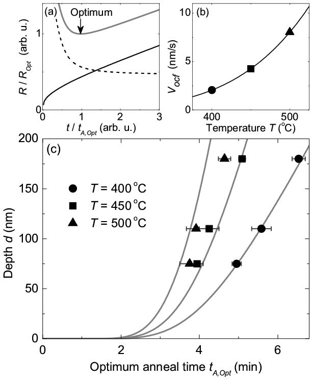
where is the local Ge concentration at depth as in Eq. 1, and where the integral runs from the depth of the Au and Ni grains to the depth of the 2DEG. The behavior of this equation is that first rapidly decreases, and then curves off to saturate at a level that is proportional to (dashed curve in Fig. 3a).
To model , we assume that the increase in resistance for over annealed contacts is related to the decrease in Ni-grain– interface area. Imagine, for simplicity, a single, square shaped Ni-rich grain with area . We model the reduction of this area as a sideways diffusion process of Au, again with a time-dependence as simple diffusion analogues to Eq. 1. The length of a side is then reduced as , where is the initial grain size, and the diffusion constant for this process, such that
| (4) |
For a very wide parameter range, this model gives that increases more or less linearly in time (solid black curve in Fig. 3a). A resistance increase that is much stronger than linear only sets in when the total interface area approaches zero, when the contact is already strongly over annealed. The total contact resistance is the sum of and (gray solid curve Fig. 3a), and the optimal annealing time is then defined as the time where this sum shows a minimum value.
We can reduce the number of fitting parameters for this modeling to only two with the following approach. For in Eq. 3, we assume parameters where saturates at a value below, but on the order of the optimal contact resistance . We also assume that this saturation occurs in a time scale on the order of a few times the optimal annealing time. For in Eq. 4, we assume that it has a value below for , and that it increases more or less in a linear fashion to a value of order . This increase should take place in a time scale on the order of the optimal annealing time. Numerically investigating this model then shows that it has for a very wide parameter range the behavior that the increase of optimal annealing time with increasing 2DEG depth is close to linear. We can express this using an effective velocity for optimal contact formation ,
| (5) |
Furthermore, numerical investigation of the temperature dependence shows that behaves according to
| (6) |
when the diffusion processes that underlie Eq. 3 and Eq. 4 are both thermally activated with a similar activation energy . We can now fit this model to our experimental data only using Eq. 5 and Eq. 6, such that we only have and as fitting parameters. In doing so, we take again into account that the temperature is not constant during annealing, and use again profiles as in Fig 1a.
The results of this fitting are presented in Fig. 3c, and as a function of temperature for these fitting parameters ( and ) is plotted in Fig. 3b. While it is a crude model, the fits are very reasonable, showing that the model is useful for predicting optimal annealing times. Furthermore, the value for is a realistic number [31, 32, 33]. Our model also predicts that the minimum value of the resistance that can be achieved for optimally annealed contacts increases with increasing 2DEG depth. We did not observe such a clear trend, probably because the resistance of optimal contacts is so low that one needs to include contributions from 2DEG square resistance around and underneath the contact when evaluating absolute values (further discussed below).
VII Contact-shape dependence
Our model for the annealing mechanism implies that optimal contacts have a rather uniform Ge concentration throughout the layers, and that this results in a value for of order 10 . This implies that the bulk resistivity in the doped Ge-doped layer is around 4 . In turn, this implies that in-plane electron transport under an optimal contact from the metallization on the surface to 2DEG on the side of the contact still mainly takes place in the original 2DEG layer. If the square resistance for transport in the original 2DEG layer below the contact does not strongly increase during annealing, and if it is smaller than the contact resistance, this also implies that the resistance of optimal contacts should be inversely proportional to the contact area. Thus, measuring whether the contact resistance depends on contact area or on the circumference of a contact can give further insight in the annealing mechanism and contact properties.
We carried out such a study, by varying the shape of contacts. All results that we discussed up to here were obtained with square contacts with an area of 0.04 and a circumference of 0.8 mm (on the side of a Hall bar). For the dependence on contact shape, we measured various sets where we varied the circumference while keeping the area constant at 0.04 , and various sets where we varied the area while keeping the circumference constant at 0.8 mm. We varied the shape from smooth circular shape to square shapes with a zig-zag edge at the 50 micronscale, to avoid getting too much resistance contribution from square resistance of 2DEG right next to a contact (for these devices we used electron-beam lithography). The study only used wafer A. All contacts were fabricated and annealed in one single batch to ensure that it is meaningful to compare the values of contact resistance.
For this study, we inject again current into the contact that is measured, and extract the current using another contact. However, the dependence on contact shape can only give an unambiguous result if the resistance from each side of the studied contact to the place in the 2DEG where the current is extracted is sufficiently similar. This can be achieved by making the distance between the contacts larger than the size of the contacts. Thus, we now fabricated contacts in the middle of 2 mm by 3 mm cleaved wafer pieces (two rows of four contacts, with center-to-center distance between rows 1 mm, and center-to-center distance between contacts within a row 0.6 mm). Using four different contacts for a 4-terminal measurement on the 2DEG (with the current biased from one row to the other) gives on these samples indeed low values around 8 , in reasonable agreement with the value of the 2DEG square resistance of about 20 . Contact resistance values were again determined in a current-biased 4-terminal configuration, with two terminals connected to the bond wire on the contact, the second current terminal on the opposite contact in the other row, and the second voltage terminal on a neighboring contact in the same row.
On contacts that are not annealed, we can observe a tunnel current, as expected for Schottky barriers. Here, the effective resistance is inversely proportional to area. For optimally annealed contacts, we found that the contact resistance was independent on circumference, while only showing a weak dependence on area (weaker than inversely proportional to area), see Fig. 4. The fact that the dependence on shape does here not show a clear dependence as agrees with the fact that the values are comparable to the square resistance of the 2DEG, such that the latter gives a significant contribution to the total contact resistance. Fully understanding the contact resistance then requires incorporating all square resistance contributions from underneath and around the 2DEG. Since we found it impossible to estimate these effects with a small error bar, we tried to demonstrate a clear dependence on area by measuring slightly under annealed contacts instead.

On two sets of under annealed contacts on wafer A, where we used shorter anneal times than (average contact resistance of 30 and 500 ), we found (within error bar) no dependence on area or circumference. We can only explain this result if we assume that the 2DEG square resistance underneath the contact is significantly increased (to values comparable to the total observed contact resistance) for under annealed contacts. This probably results from the in-diffusing Ge (and atomic Au and Ni [15, 27]), which already introduces strain and scatter centers in the 2DEG layer before optimal contact conditions are reached. For optimal annealed contacts (here with total resistance of typically 7 , independent of circumference), the square resistance underneath a contact must have returned to a low value of order 10 . Apparently, the resistance increase due to strain and scatter centers is compensated by increased Ge doping near the 2DEG layer.
The summary of this study is that the resistance of annealed contacts never shows in a clear dependence on circumference, and only a weak dependence on area for optimal contacts. We can, nevertheless, draw the following conclusions. For an optimal ohmic contact, it is not the case that electron transport between the surface metallization and the surrounding 2DEG mainly occurs at the edge of a contact. Instead, the full contact area plays a role, and in-plane electron transport under an optimal contact mainly takes place in the original plane of the 2DEG. In addition, we find it impossible to evaluate the absolute values of the contact resistance of our devices with an accuracy within a factor 2, since the resistance of an optimal contact has a contribution from the square resistance underneath the contact, and its value is influenced by the annealing process. Further, future studies in this direction should consider that pressing the bond wire (with a footprint of about 100100 ) onto the surface metallization may locally disturb the contact properties, which can disturb a clear dependence on contact shape.
We could therefore not study the property of our model that the optimal contact resistance value should be proportional to . Instead, we should evaluate whether the enhanced square resistance underneath a contact needs to be incorporated in our model. We find that this is not needed for the following reasons: for over annealing it does not play a role, since we observe the same over-annealing mechanism as observed on bulk n-GaAs. Optimally annealed contacts occur when the square resistance underneath the contacts has again low values of order 10 . Here we observe a weak area dependence and no dependence on circumference, such that we can rule out that the effect dominates the contact resistance. Thus, the only effect is that it temporarily enhances the total contact resistance by about a factor 2 while the annealing progresses towards optimal contact conditions. Note that this does not change the fact that lowering the contact resistance in this phase still fully depends on further Ge diffusion towards the 2DEG layer. Therefore, it only slightly modifies how in Eq. 3 decreases towards low values.
VIII Conclusions
Summarizing, we have measured the zero-bias resistance of annealed AuGe/Ni/Au ohmic contacts to a 2DEG as a function of annealing time and temperature. We have thus obtained optimal annealing parameters for three different heterostructures where the 2DEG lies at a different depth below the wafer surface. TEM images of several annealed contacts provided further insight into the annealing mechanism and the formation of a good ohmic contact.
Combining this information we have developed a model that can predict the optimal annealing parameters for contacting a 2DEG at a certain depth in a GaAs/ heterostructure. The model assumes two competing processes: 1) Diffusion of Ge into the heterostructure lowers the contact resistance, and results in linear transport characteristics. 2) At longer annealing times, Au-rich phases diffuse in between the heterostructure and Ni-rich phases at the wafer surface. The associated increase in contact resistance is probably due to subsequent diffusion of Ga into this Au-rich phase, since this increases the number of Ga vacancies in the heterostructure near the metallization on the surface. The competition between these two processes results in a mechanism where the optimal annealing time (for a process at constant annealing temperature) is proportional to the depth of the 2DEG below the surface, and the speed of this process has thermally activated behavior. This model should have predictive power for many heterostructures, as long as the temperature of the samples as a function of time during the annealing process is known. Our study of how the contact resistance depends on the shape of the contact confirmed that the full contact area plays a role in electron transport between the metallization on the surface and the 2DEG.
Our model may become invalid for systems with a very deep 2DEG, since (Eq. 4) is expected to increase more rapidly at long annealing times, possibly resulting in non-ohmic behavior. Our results suggests that for solving this problem the focus should be at maintaining sufficient contact area between Ge-rich Ni grains and the Ge-doped layer at long annealing times. This can possibly be engineered by changing the layer thickness, order and composition of the initial AuGe/Ni/Au metallization [19, 12, 14, 15, 16, 21, 26], or by including a Pt, Nb or Ag layer below the top Au layer that suppresses the intermixing of this Au with layers at the wafer surface[7, 19, 15, 22, 24] (uniform Ni/Ge/As layers been reported [21]). Alternatively, one can reduce the depth of the 2DEG by etching before deposition of AuGe/Ni/Au (up to the point where this results in depletion of the 2DEG).
ACKNOWLEDGMENTS
We thank B. H. J. Wolfs, M. Sladkov and S. J. van der Molen for help and valuable discussions. Further, we acknowledge the Dutch Foundation for Fundamental Research on Matter (FOM), the Netherlands Organization for Scientific Research (NWO), and the German programs DFG-SFB 491 and BMBF-nanoQUIT for funding.
References
- [1] See for example: C. W. J. Beenakker and H. van Houten, Solid State Physics 44, 1 (1991).
- [2] See for example: L. L. Sohn, L.P. Kouwenhoven, and G. Schön, eds., Mesoscopic Electron Transport, NATO ASI Series E 345 (Kluwer, Dordrecht, Netherlands, 1997).
- [3] For a review see: A. G. Baca, F. Ren, J. C. Zolper, R. D. Briggs, and S. J. Pearton, Thin Solid Films 308-309, 599 (1997).
- [4] N. Braslau, J. B. Gunn, and J. L. Staples, Solid-State Electron. 10, 381 (1967).
- [5] M. Ogawa, J. Appl. Phys. 51, 406 (1980).
- [6] N. Braslau, J. Vac. Sci. Technol. 19, 803 (1981).
- [7] C. P. Lee, B. M. Welch, and J. L. Tandon, Appl. Phys. Lett. 39 556 (1981).
- [8] M. Heiblum, M. I. Nathan, and C. A. Chang, Solid-State Electron. 25, 185 (1982).
- [9] T. S. Kuan, P. E. Batson, T. N. Jackson, H. Rupprecht, and E. L. Wilkie, J. Appl. Phys. 54, 6952 (1983).
- [10] N. Braslau, Thin Solid Films 104, 391 (1983).
- [11] N. Braslau, J. Vac. Sci. Technol. A 4, 3085 (1986).
- [12] M. Procop, B. Sandow, H. Raidt, and L. D. Son, Phys. Stat. Sol. A 104, 903 (1987).
- [13] J. R. Waldrop and R. W. Grant, Appl. Phys. Lett. 50, 250 (1987).
- [14] R. A. Bruce and G. R. Piercy, Solid-State Electron. 30, 729 (1987).
- [15] J. R. Shappirio, R. T. Lareau, R. A. Lux, J. J. Finnegan, D. D. Smith, L. S. Heath, and M. Taysing-Lara, J. Vac. Sci. Technol. A 5, 1503 (1987).
- [16] E. Relling and A. P. Botha, Appl. Surf. Scie. 35, 380 (1988).
- [17] V. G. Weizer and N. S. Fatemi, J. Appl. Phys. 64, 4618 (1988).
- [18] N. E. Lumpkin, G. R. Lumpkin, and K. S. A. Butcher, J. Mater. Res. 11, 1244 (1996).
- [19] P. Zwicknagl, S. D. Mukherjee, P. M. Capani, H. Lee, H. T. Griem, L. Rathbun, J. D. Berry, W. L. Jones, and L. F. Eastman, J. Vac. Sci. Technol. B 4 476 (1086).
- [20] T. K. Higman, M. A. Emanuel, J. J. Coleman, S. J. Jeng, and C. M. Wayman, J. Appl. Phys. 60, 677 (1986).
- [21] A. K. Rai, A. Ezis, R. J. Graham, R. Sharma, and D. W. Langer, J. Appl. Phys. 63, 4723 (1988).
- [22] Y. Jin, Solid-State Electron. 34, 117 (1991).
- [23] R. P. Taylor, P. T. Coleridge, M. Davies, Y. Feng, J. P. McCaffrey, and P. A. Marshall, J. Appl. Phys. 76, 7966 (1994).
- [24] A. Messica, U. Meirav, and H. Shtrikman, Thin Solid Films 257, 54 (1995).
- [25] R. P. Taylor, R. Newbury, A. S. Sachrajda, Y. Feng, P. T. Coleridge, M. Davies, and J. P. McCaffrey, Superl. Microstr. 24, 337 (1998).
- [26] S. Raiser, U. Graumann, M. Fleischer, J. Schmid, S. Jauerneck, J. Weis, and D. A. Wharam, Scientific program of the 2005 German DPG meeting, abstract HL 58.67 (unpublished); http://www.dpg-tagungen.de/archive/.
- [27] G. Sai Saravanan, K. Mahadeva Bhat, K. Muraleedharan, H. P. Vyas, R. Muralidharan, and A. P. Pathak, Semicond. Sci. Technol. 23, 025019 (2008).
- [28] The work that we cite in the introduction shows that the lowest values for contact resistance to n-GaAs and 2DEG systems with only a thin (few nm) buffer layer (undoped between doping and the 2DEG) are of order 0.1 , giving 0.5 for 0.2 mm wide contacts. However, 2DEG systems with the thickness of the buffer layer in the range of 35 nm typically give values that are an order of magnitude higher [22]. Note that values are often reported in units , which is not representing the bulk resistivity between surface metallization and 2DEG, but representing the contact resistance normalized to contact width, as derived with the TLM method [29, 30].
- [29] H. H. Berger, Solid-State Electron. 15, 145 (1972).
- [30] G. K. Reeves and H. B. Harrison, IEEE Electron Device Lett. 3, 111 (1982).
- [31] K. Sarma, R. Dalby, K. Rose, O. Aina, W. Katz, and N. Lewis, J. Appl. Phys. 56, 2703 (1984).
- [32] A. K. Kulkarni and C. Lai, J. Vac. Sci. Technol. A 6, 1531 (1988).
- [33] A. K. Kulkarni and C. Lai, Thin Solid Films 164, 435 (1988).
- [34] Early in the annealing process, the grains mainly containing Ni and Ge have been identified as , and phases [9, 12].
- [35] It is believed that the height of the Schottky barrier is under all relevant conditions pinned at about 0.8 eV [11]. A lowering of the Schottky barrier with Au, Ni and Ge layers on the wafer surface was only observed for very specific interfaces [13], and does probably not occur during actual annealing of AuGe/Ni/Au contacts [12].