Elementary Charge Transfer Processes in Mesoscopic Conductors
Abstract
We determine charge transfer statistics in a quantum conductor driven by a time-dependent voltage and identify the elementary transport processes. At zero temperature unidirectional and bidirectional single charge transfers occur. The unidirectional processes involve electrons injected from the source terminal due to excess dc bias voltage. The bidirectional processes involve electron-hole pairs created by time-dependent voltage bias. This interpretation is further supported by the charge transfer statistics in a multiterminal beam splitter geometry in which injected electrons and holes can be partitioned into different outgoing terminals. The probabilities of elementary processes can be probed by noise measurements: the unidirectional processes set the dc noise level while bidirectional ones give rise to the excess noise. For ac voltage drive, the noise oscillates with increasing the driving amplitude. The decomposition of the noise into the contributions of elementary processes identifies the origin of these oscillations: the number of electron-hole pairs generated per cycle increases with increasing the amplitude. The decomposition of the noise into elementary processes is studied for different time-dependent voltages. The method we use is also suitable for systematic calculation of higher-order current correlators at finite temperature. We obtain current noise power and the third cumulant in the presence of time-dependent voltage drive. The charge transfer statistics at finite temperature can be interpreted in terms of multiple charge transfers with probabilities which depend on energy and temperature.
pacs
72.70.+m, 72.10.Bg, 73.23.-b, 05.40.-aI Introduction
The charge transmitted through a mesoscopic conductor during a fixed time interval fluctuates because of charge discreteness and stochastic nature of transport. The objective of the statistical theory of quantum transport, full counting statistics, is to completely characterize the probability distribution of transferred charge. The field of full counting statistics has attracted significant attention because it provides the most detailed information on charge transfer accessible in the measurements of the average current, current noise power,[1] and higher-order current correlations.[2, 3, 4]
The problem of full counting statistics has been addressed first by Levitov and Lesovik[5, 6] for the case of dc biased multiterminal junctions and subsequently generalized to a time-dependent voltage bias.[7, 8] In addition to the scattering theory of Levitov and Lesovik (see also Ref. 9), the theoretical approaches to full counting statistics include the so-called stochastic path-integral approach[10, 11] and the quantum-mechanical theory based on an extension of the Keldysh-Green’s function technique.[12, 13, 14, 15, 16] Although equivalent, these theories provide different methods to access the charge transfer statistics. Using the extended Keldysh-Green’s functions technique, the theory of full counting statistics of a general quantum-mechanical observable has been formulated,[17, 18] including the effects of a detector back action.[19] The problem of quantum measurement in the context of full counting statistics of non-commuting spin observables has also been analyzed.[20, 21] The discretization[22, 23] in space of the Keldysh-Green’s functions results in a quantum circuit theory[24, 26, 25] which greatly simplifies the calculations. The circuit theory can describe junctions with different connectors and leads, as well as multiterminal circuits.[27]
The goal of evaluation of full counting statistics in mesoscopic conductors has essentially been accomplished: the aforementioned theories provide methods and techniques to calculate the cumulant generating function of transferred charge from which the probability distribution can be obtained. However, the interpretation of the resulting statistics is often not straightforward. This is because the total statistics are composed of many electrons injected towards conductor, each exhibiting different chaotic scattering and multiple reflections before entering an outgoing terminal. At finite temperatures, the charge flow is bidirectional with both injection and absorption of electrons from terminals. The particle correlations due to Pauli principle, interactions, and those induced by the superconducting and/or ferromagnetic proximity effect also affect the charge transfer statistics.
To understand the statistical properties of collective charge transfer, one has to find the independent elementary processes constituting the statistics. The independent processes can be revealed by decomposition of the total cumulant generating function into a sum of simpler ones. The physical interpretation obtained this way goes beyond information contained in the average current, noise, and finite-order cumulants, and pertains to all transport measurements. For example, the elementary processes in a dc biased normal junction are single-electron transfers, which are independent at different energies. At finite temperatures, the electrons are transferred in both directions with correlated left- and right-transfers. At low temperatures only unidirectional electron transfers remain, with direction set by polarity of applied voltage. The elementary processes in a superconductor/normal contact are single- and double-charge transfers.[28, 24] At low temperatures and voltages below the superconducting gap only double-charge Andreev processes remain, while above the gap normal single-charge transfers dominate. The elementary charge transfer processes between superconductors with dc bias applied consist of multiple charge transfers due to multiple Andreev reflections. [29, 30, 31, 32] The interpretation of elementary charge transfer processes between superconductors with constant phase difference is more subtle. In this case charge transfers acquire formally negative probabilities and the proper physical interpretation has to include dynamics of a detector. [13, 17, 18]
In contrast to dc voltage bias, time-dependent voltage drive mixes electron states of different energies which in combination with the Pauli principle leads to a nontrivial charge transfer statistics. The signatures of this statistics have been studied first through the noise in an ac-driven junction (photon-assisted noise).[33, 34] The photon-assisted noise at low temperatures is a piecewise linear function of a dc voltage offset with kinks corresponding to integer multiples of the driving frequency and slopes which depend on the amplitude and shape of the ac component. This dependence has been observed experimentally in normal coherent conductors[36, 35] and diffusive normal metal/superconductor junctions.[37] The photon-assisted noise at small driving amplitudes is due to an electron-hole pair which is created by ac drive (with a low probability per voltage cycle) and injected towards the scatterer.[38, 39, 40] However, to obtain the elementary processes, the knowledge of full charge transfer statistics is needed.
The elementary processes in the presence of time-dependent drive have been identified in Refs. 42, 41, 43 for the special choice of a driving voltage. The authors have studied Lorentzian voltage pulses of the same sign carrying integer numbers of charge quanta. In this case the elementary processes are electrons injected towards the scatterer without creation of the electron-hole pairs. The charge transfer is unidirectional with binomial statistics set by the effective dc voltage. This result is independent of the relative position of the pulses, their duration, and overlap. The many-body quantum state generated by these pulses has been obtained recently.[43] An alternative way to inject single electrons free of electron-hole pairs is by using time-dependent shifts of a resonant level in a quantum dot.[44, 45, 46, 47, 48]
The elementary charge transfer processes for arbitrary time-dependent voltage drive have been identified in Ref. 49. At low temperatures these processes are single-charge transfers which originate from electrons and electron-hole pairs injected towards the scatterer. The electrons are injected due to excess dc voltage applied and give a binomial contribution to the total cumulant generating function. The electron-hole pairs are created by the ac component of the voltage drive. The probabilities of pair creations per voltage cycle depend on the details of the ac drive. For the special choice of optimal Lorentzian voltage pulses no electron-hole pairs are created. In general, however, an ac drive does create electron-hole pairs, with more and more pairs created per voltage cycle as the amplitude of the drive increases. A geometric interpretation of elementary processes is studied in Ref. 50. For time-dependent scatterer, the constraints imposed on charge transfer statistics restrict the allowed charge transfers.[51]
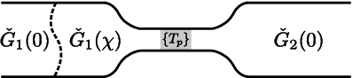
In this article we present a comprehensive study of elementary processes in a generic mesoscopic conductor in different physical regimes, as depicted in Fig. 1.

We first obtain the cumulant generating function for a coherent voltage-driven quantum contact at finite temperatures, using both the formalism of Levitov and Lesovik and the circuit theory of quantum transport (Sec. II). We then identify the elementary charge transfer processes at zero temperature (Sec. III.1). Decomposition of the noise into contributions of elementary processes for different voltage signals is studied in Sec. III.2. For ac voltage drive, the differential noise oscillates as the amplitude of the drive increases due to new electron-hole pairs being created per voltage cycle. The number of electron-hole pairs per cycle becomes large for driving amplitudes much larger than frequency. In this case the statistics in the leading order reduces to uncorrelated electron and hole transfers and depends on an effective voltage only, independent of the details of the ac drive. The elementary processes can be probed also for both ac and dc voltages present, e.g., in the regime in which the ac component of the drive is kept fixed and the dc offset changes. In this case both the electrons and created electron-hole pairs are injected towards the junction. The electron-hole pairs give rise to the excess noise with respect to the noise level set by dc voltage offset.
The notion of elementary processes, being a matter of interpretation of the full charge transfer statistics, provides physically plausible and intuitive description of transport in terms of statistically independent events. Such a description persists in all transport measurements. For example, the picture of electrons and electron-hole pairs injected towards the scatterer, which we have inferred from a study of a 2-terminal junction, is further supported by the evaluation of the full counting statistics in a beam-splitter geometry in which case the injected particles can be separated into different outgoing terminals. These processes can be probed by current cross correlations (Sec. III.3).
The method we use is also suitable for systematic calculation of the higher-order current correlators at finite temperature. The current noise power and the third cumulant in the presence of time-dependent voltage drive are obtained in Sec. IV. The interpretation of the full counting statistics and the elementary processes are fundamentally different at finite temperature. For a periodic drive, the elementary processes are transfers of multiple integer charge quanta with probabilities which depend on energy and temperature (Sec. V).
II Cumulant generating function
The system we consider is a generic 2-terminal mesoscopic conductor characterized by a set of transmission eigenvalues . For a large number of channels, the transport properties are universal and independent of microscopic details of geometry of the junction and positions of impurities. We can neglect the energy dependence of transmission eigenvalues if the the electron dwell time is small with respect to time scales set by the inverse temperature and applied voltage. The cumulant generating function of the transferred charge is given by determinant formula[5, 41, 52]
| (1) |
where
| (2) |
Here is the matrix of occupation numbers of the terminals which is diagonal in the terminal indices and scalar in transport channels, is the scattering matrix of the junction, and is the transformation which incorporates the counting fields. Because the current is conserved, it is sufficient to assign only one counting field to the left terminal. We count charges which enter the left terminal irrespective the channel, the energy, or the spin, with being scalar in the corresponding indices. The determinant in Eq. (1) is taken with respect to the terminal, channel, energy, and spin indices.
The occupation numbers and of the left and right terminals are matrices in energy indices and scalars in channel and spin indices. In the case of dc voltage bias are diagonal in energy with , where , is the voltage applied, and is the electronic temperature. In the presence of time-dependent drive the occupation numbers are not diagonal in energy indices and do not commute. The voltage drive can be incorporated via the gauge transformation in time representation with , where we assume the convolution over internal time indices.
Equation (1) can be simplified using polar decomposition of the scattering matrix [53]
| (3) |
Here , , , and are unitary matrices in transport channels and and are diagonal matrices of transmission and reflection eigenvalues. Equation (1) for the 2-terminal junction reduces to
| (4) |
where takes into account the spin degree of freedom. Since the operators in the first (the second) row commute, the determinant can be calculated blockwise. Using Eq. (34) given in Appendix we obtain
| (5a) | ||||
| (5b) | ||||
Here we used the matrix identity and the trace is taken in energy indices. The logarithm is taken assuming convolution over internal energy indices, e.g., .
In the following we show that the same result is obtained within the circuit theory of mesoscopic transport.[24, 26, 25] In this case the system is represented by discrete circuit elements as depicted in Fig. 2.
The cumulant generating function of the transferred charge is given by[22, 16]
| (6) |
where
| (7) |
are the quasiclassical Keldysh-Green’s functions of the terminals with . The counting field is incorporated through the gauge transformation of the Keldysh-Green’s function of the left terminal,
| (8) |
where
| (9) |
in Keldysh space. The logarithm and the trace in Eq. (6) are taken assuming the convolution both in Keldysh and in energy indices.
Equation (6) can be simplified by using matrix representation in Keldysh space. After rewriting and taking the determinant by blocks using Eq. (34), the result coincides with Eq. (5). This proves the equivalence of the circuit-theory expression for [Eq. (6)] and the Levitov determinant formula [Eq. (1)] for a coherent 2-terminal scatterer. The circuit-theory approach becomes advantageous in the case of several scatterers in series[23, 54] or for a multiterminal mesoscopic conductor with large number of conduction channels.[27] It gives the charge transfer statistics in terms of the scattering properties of individual elements, thus circumventing a non-trivial task of obtaining the scattering matrix of the composite system and averaging over the phase shifts.
Equation (5) is valid for a dc bias applied and energy-dependent transmission probabilities. In this case the occupation numbers are diagonal in energy and commute with each other and with . The trace over energy reduces simply to the integration and we obtain
| (10) |
Here is the measurement time which is the largest time scale in the problem, much larger than the characteristic time scale on which the current fluctuations are correlated.[55] The form of reveals that the elementary charge transfer processes are single-electron transfers to the left and to the right. The electron transfers at different energies and in different channels are independent. The term in Eq. (10) describes the electron transfer from the right to the left lead at energy in the channel . The probability of this process is proportional to the probability that the state in the right lead is occupied, the probability that the state in the left lead is empty, and the probability of transfer across the scatterer. A similar analysis holds for the electron transfer from left to right. The left and right transfers are correlated because is not a sum of the left- and right-transfer generating functions.
Equation (5) is also valid for the time-dependent voltage applied and energy-independent transmission probabilities. In this case do not commute with each other. [However, the order of and can be exchanged as shown by Eqs. (5a) and (5b).] The logarithm has to be calculated with the matrix structure of in energy indices taken into account because time-dependent drive mixes the electron states with different energies.
A few remarks on applicability of our approach are in place here. The circuit theory we have used applies to instantaneous scattering at the junction, with the frequency of the bias voltage much smaller than the inverse dwell time . It also applies for a dot sandwiched between 2 terminals and much smaller than the inverse time of the charge relaxation on the dot. In a typical experimental situation ,[56, 57] with limited by the dwell time . However, as shown in Ref. 39, the photon-assisted noise in the leading order in driving amplitude does not depend on : in a weakly-driven junction the frequency range is set by the time, . The dwell time becomes important for larger voltage amplitudes. For a maximum in develops at the frequency because the photon-assisted noise probes the electronic distribution function which relaxes on a timescale given by .[56, 57] At frequencies , the differential noise as a function of is increased with respect to the case . The increase is of the order of with the distances between maxima and minima only weakly affected. This is consistent with the experiments of Schoelkopf et al. [36] and Kozhevnikov et al. [37] which can be described by assuming the instantaneous scattering even though the frequency of the ac signal applied is comparable or larger than the inverse dwell time.
III Elementary charge transfer processes at
III.1 Decomposition of the cumulant generating function into elementary processes
In this section we study elementary charge transfer processes in a 2-terminal junction with constant transmission eigenvalues and time-dependent voltage applied. The cumulant generating function is given by Eq. (5). To identify the elementary processes we diagonalize the operator under the logarithm in energy indices. As a first step, we rewrite Eq. (5b) in terms of and :
| (11) |
where and .[58] The further simplifies in the zero temperature limit, in which the hermitian -operators are involutive , and satisfy . Thus the eigensubspaces of are invariant with respect to , , and , and the diagonalization problem reduces to the subspaces of lower dimension. The typical eigensubspaces of are 2-dimensional and spanned by the eigenvectors and of which correspond to the eigenvalues ( is real). The diagonalization procedure in invariant subspaces is described in detail in Ref. 49.
For computational reasons it is convenient to impose periodic boundary conditions on the voltage drive with the period . In this case the operator couples only energies which differ by an integer multiple of . This allows to map the energy indices into the interval while retaining the discrete matrix structure in steps of . The operator in energy representation is given by
| (12) |
with
| (13) |
Here is the dc voltage offset and is the ac voltage component. The coefficients satisfy
| (14) |
The cumulant generating function at zero temperature is given by with[49]
| (15) |
and
| (16) |
Here , , and , where is the largest integer less than or equal . The coefficient in Eq. (16) is related to direction of the charge transfer, with () for (). The total measurement time is much larger than the period and the characteristic time scale on which the current fluctuations are correlated.
The parameters in Eq. (15) depend on the details of the time dependent voltage drive. They are given by , where are the eigenvalues of calculated for []. The eigenvalues are obtained using a finite-dimensional matrix , with the cutoff in indices and being much larger than the characteristic scale on which vanish.
Equations (15) and (16) give the charge transfer statistics in a 2-terminal junction driven by a time-dependent voltage. The result is valid in the zero-temperature limit, with no thermal excitations present. The probability distribution of the number of charges transferred within measurement time is given by . The cumulants of are given by and are related to the higher-order current correlators at zero frequency.[17, 18] For example, the average current, the current noise power, and the third cumulant of current fluctuations are given by , , and , respectively.[59]
The elementary charge transfer processes can be identified from the form of , similarly as in Refs. 60 and 61. The result is depicted schematically in Fig. 3.

The describes unidirectional single-electron transfers due to the excess dc bias voltage applied. The number of attempts for an electron to traverse the junction within measurement time is given by (we take into account both spin orientations). The transfer events in different channels are independent. The term in Eq. (16) describes a single-electron transfer with probability in th channel. The unidirectional charge transfer processes give contributions to the average current and higher-order cumulants.
The and describe bidirectional charge transfer processes. Different bidirectional processes are labelled by in Eq. (15). These processes represent electron-hole pairs created in the source terminal by the time-dependent voltage drive and injected towards the scatterer. The probability of such an electron-hole pair creation is given by and depends on the details of the ac voltage component . The charge transfer in th channel occurs if one particle (e.g., electron) is transmitted and the hole is reflected, or vice versa. The probability for the whole process is given by . The bidirectional processes contribute to the noise and higher-order even cumulants. However, they give no contributions to the average current and higher-order odd cumulants because electrons and holes are transmitted with the same probability.
The two types of bidirectional processes and differ in the number of attempts and have different probabilities . The depend on the number of unidirectional attempts per period per spin. The simplest statistics is obtained for an integer value of for which vanishes, in agreement with Ref. 7.
III.2 Comparison of different time-dependent voltages
The elementary processes at zero temperature can be probed by noise measurements. In what follows we compare the elementary processes and the noise generated by different time-dependent voltages. We focus on standard periodic voltage signals such as cosine, square, triangle, and sawtooth. We also present results for Lorentzian voltage pulses which provide the simplest charge transfer statistics for certain amplitudes. The applied voltage is characterized by coefficients given by Eq. (13). These coefficients are calculated explicitly in Sec. B in Appendix for the driving voltages of interest.
We first consider ac voltage drive with no dc bias applied, . In this case only the bidirectional processes of R-type remain, . The number of attempts during the measurement time is given by which corresponds to a single attempt per voltage cycle per spin. The current noise power is given by
| (17) |
with the probabilities of electron-hole pair creations obtained from the eigenvalues of , as discussed in Sec. III.1.
The probabilities for the harmonic voltage drive are shown in Fig. 4(a).

As the amplitude increases the probabilities also increase and new pairs start to enter the transport. This results in the oscillatory change of the slope of as a function of . The decomposition of the differential noise into elementary processes is shown in Fig. 4(b). The differential noise for different time-dependent voltages is shown in Fig. 5 for comparison.

The bidirectional processes with the unit probability represent electron-hole pairs which are created and injected towards the scatterer in each voltage cycle. In this case the electron and hole transfers are statistically independent. This can be seen from the corresponding cumulant generating function which reduces to , where describe electron and hole transport. The electron-hole pairs which are created with the probability result in correlated electron and hole transfers. The corresponding cumulant generating function is given by and cannot be partitioned into independent electron and hole contributions.
The interpretation of the shot noise in terms of electron-hole pair excitations has been studied previously in Ref. 38 in the regime of low-amplitude harmonic driving . In this case only one electron-hole pair is excited per period with probability . Remarkably, Fig. 4 shows that the single electron-hole pair is excited not only for small amplitudes but also for amplitudes comparable or even larger than the drive frequency. This extended range of validity can be covered by taking into account the higher-order terms in the expression for probability , where denote Bessel functions (cf. Sec. IV). The first terms approximate the exact shown in Fig. 4 to accuracy better than for .
For large driving amplitudes the charge transfer statistics does not depend on the details of time-dependent drive[8, 42] and can be characterized by an effective voltage (here we assume ). In this case there are processes with . The charge transfer statistics in the leading order in consists of uncorrelated electrons and holes injected towards the contact in each transport channel during measurement time: . This result can be interpreted by comparison with the generating function of a dc bias given by Eq. (16). The electrons (holes) are injected during time intervals () per voltage cycle in which []. For a large number of injected particles, the time-dependent drive in these intervals can be replaced by effective dc voltages and . The number of attempts is given by ( e, h), in agreement with Eq. (16). The noise generated is the sum of independent electron and hole contributions . This explains the asymptotic behavior of differential noise at large driving amplitudes shown in Figs. 4 and 5.

In the following we consider time-dependent voltage drive with a nonzero dc offset which creates both unidirectional and bidirectional elementary processes. The unidirectional processes generate dc noise which is given by . The bidirectional processes given by Eq. (15) generate the excess noise :
| (18) |
where is the fractional part of . For there are 2 types of bidirectional processes (labelled by L and R) with different number of attempts and different probabilities of electron-hole pair creations.
We study bidirectional processes first in the regime in which the ac amplitude and the dc offset increase simultaneously. The excess noise for different time-dependent voltages is shown in Fig. 6(a) for comparison. The probabilities as a function of voltage are shown in Fig. 6(b) for the cosine voltage drive. The decomposition of the excess noise into contributions of elementary processes is shown in Fig. 6(c). For the cosine voltage drive there are 2 bidirectional processes (one of L-type and another of R-type) which are excited per period. The L-type processes transform continuously into the R-type ones at integer values of , while the R-type processes disappear. The step-like evolution of the probabilities of R-type processes as a function of voltage does not introduce discontinuities in the current noise because the corresponding number of attempts vanishes. Instead, the interplay between L- and R-processes results in kinks and the local minima at integer values of , as shown in Fig. 6(a). The L-type (R-type) processes give the dominant contributions as approaches the integer values from the left (right) because of the number of attempts which is proportional to ().
The Lorentzian voltage drive is special because it provides the simplest one-particle charge transfer statistics. This is achieved for impulses carrying an integer number of charge quanta at offset voltages . In this case the Lorentzian pulses do not create electron-hole pairs and only single-particle processes given by Eq. (16) remain. The charge transfer statistics in each transport channel is exactly binomial.[42, 41] The noise is reduced to the minimal noise level of the effective dc bias, as shown in Fig. 6(a). A formal reason for this is the vanishing of the coefficients for [cf. Eqs. (29) and (42)]. A many-body state which is created by optimal Lorentzian pulses has been obtained by Keeling et al.[43] recently.

Now we focus on regime in which the ac component of the drive is fixed and the dc offset changes. At low temperatures, the shot noise is a piecewise linear function of the dc voltage offset with kinks corresponding to integer multiples of the driving frequency and slopes which depend on the shape and the amplitude of the ac voltage component.[33, 34] The differential noise consists of a series of steps, as shown in Fig. 7(a). The piecewise linear dependence of noise can be understood in terms of probabilities of elementary processes.[7] For the ac component fixed, the probabilities and of electron-hole pair creations are piecewise constant as a function of , and can be re-labelled by and where . This results in the piecewise linear dependence of the excess noise given by Eq. (18) as a function of . For the dc offset in the interval with integer, the excess noise is a linear combination of processes and () with the number of attempts proportional to and , respectively. For a different set of processes and contributes and the excess noise changes slope. The excess noise for harmonic drive is shown in Fig. 7(b) (solid line) with decomposition into contributions of elementary processes (dotted lines). The probabilities of elementary processes are shown in the inset.
III.3 Beam splitter geometry
Here we study a multiterminal beam splitter geometry depicted in Fig. 8. The source terminal is biased with a time-dependent periodic voltage and through a mesoscopic conductor attached to several outgoing terminals. The conductor is characterized by a set of transmission eigenvalues and the outgoing leads by conductances . We are interested in the limit in which the outgoing leads play a role of a detector and only weakly perturb the charge transfer across the conductor. This is achieved for the conductance to the outgoing leads much larger than the conductance of a conductor. In this case the particles which traverse the conductor enter the outgoing terminals with negligible backreflection into the source terminal. A similar setup with spin-selective outgoing contacts has been used in Ref. 61 to reveal singlet electron states.
The cumulant generating function is calculated using the circuit theory similarly as in Sec. II for the 2-terminal case. In contrast to Sec. II, here we assign the counting fields to the outgoing terminals. The Green’s function of the source terminal and the Green’s functions of the outgoing ones are given by
| (19a) | |||
| and | |||
| (19b) | |||
Here and are the matrices in energy indices defined in Sec. III.1. The Green’s function of the internal node is given by matrix current conservation and normalization condition . In the limit , the central node is strongly coupled to the outgoing terminals and the can be obtained in the lowest order with the terminal unattached. For simplicity we assume tunnel couplings to the outgoing terminals. In this case matrix current conservation reduces to[22, 24]
| (20) |

In the following we work in the low-temperature limit in which . We seek for the solution in the form where is the vector of Pauli matrices in Keldysh space. From Eqs. (19) and (20) we obtain where , , and . The cumulant generating function of the charge transferred is given by
| (21) |
where summation over the internal Keldysh and energy indices is assumed. The diagonalization of is performed along the lines of Ref. 49.
For the cumulant generating function we obtain where are the contributions of bidirectional processes and is the contribution of the unidirectional ones. The unidirectional processes are described by
| (22) |
where is the measurement time and is the dc voltage offset (here we assume ). The bidirectional processes are described by
| (23) |
Here labels the bidirectional processes, labels transport channels, and label the outgoing terminals, and . The number of attempts and the probabilities are the same as in Sec. III.1.
Equations (22) and (23) give the statistics of the charge transfer in a multiterminal beam splitter at low temperatures in the presence of a periodic time-dependent drive at the source terminal. The and have a direct physical interpretation. The unidirectional processes, which are described by , are the single-electron transfers across the structure due to the dc offset voltage applied to the source terminal. The term in Eq. (22) represents the process in which an electron in the th transport channel traverses the conductor with probability and enters the outgoing terminal with probability .
On the other hand, the bidirectional processes represent the electron-hole pairs created in the source terminal and injected towards the conductor. The probabilities of such excitations are given by . The interpretation of the cumulant generating function given by Eq. (23) can be obtained from a simple counting argument. The term in Eq. (23) represents the process in which electron-hole excitation is created, hole is reflected, and electron is transmitted into the outgoing terminal . Similarly, the term represents the process in which the electron is reflected and the hole is transmitted. Finally, the term () represents the process in which both particles are transmitted with electron entering terminal and hole entering terminal .
Charge transfer statistics and current correlations can be obtained using the cumulant generating function . For example, the current cross correlation between different terminals and is given by :
| (24) |
We find that only bidirectional processes in which both particles are transferred (one into the terminal and another into the terminal ) give the contributions to the cross correlation . This has been obtained previously by Rychkov et al. [38] in the special case of harmonic drive in the limit of small driving amplitudes ( and ).
The cross correlation depends on bidirectional processes and is proportional to the excess noise of a 2-terminal junction [Eq. (18)]. In a 2-termianal setup, the excess noise is just a small correction to generated by unidirectional processes for a bias voltage with (Fig. 6). The contribution of component can be reduced by measuring current cross correlations between different outgoing terminals in the beam splitter geometry with negligible backscattering.
IV Cumulants at
The full counting statistics and the corresponding elementary transport processes obtained in Sec. III are valid description in the low temperature limit only, in which electron-hole pairs are created by the applied voltage and no thermally excited pairs exist. Formally, the diagonalization of the operator in Eq. (11) in energy indices, which is needed to deduce the elementary processes, is based on the involution property of -operators: . This property no longer holds at finite temperatures which are comparable to the applied voltage. Nevertheless, the method we use enables the efficient and systematic analytic calculation of the higher-order cumulants at finite temperatures.
The cumulants can be obtained directly from Eq. (11) by expansion in the counting field to the certain order before taking the trace. The trace of a finite number of terms can be taken in the original basis in which and are defined. In the following we illustrate the approach by calculation of the average current, the current noise power, and the third cumulant at finite temperatures. From Eq. (11) we obtain
| (25a) | ||||
| (25b) | ||||
| (25c) | ||||
In energy representation, the operators and are given by
| (26a) | ||||
| (26b) | ||||
Here and we used the properties of given by Eq. (14). After integration over energy in Eqs. (25) we obtain the average current . The current noise power and the third cumulant are given by
| (27) |
and
| (28) |
respectively. For a dc voltage bias and the noise and the third cumulant reduce to and at zero temperature. Here is the Fano factor and .
The average current is linear in dc voltage offset, which is consistent with the initial assumption of energy-independent transmission eigenvalues and instant scattering at the contact. The result for the current noise power, Eq. (27), describes the photon-assisted noise for arbitrary periodic voltage drive. The coefficients for harmonic drive are given by the Bessel functions, , and Eq. (27) reduces to the previous results obtained by Lesovik and Levitov[33] and Pedersen and Büttiker[34] (see also Ref. 1). The accurate noise measurements at finite temperatures in the presence of the harmonic driving are performed in Ref. 35. The results are in agreement with Eq. (27).
In the following we discuss the low- and high-temperature limits of and . At high temperatures , with being the characteristic energy scale on which vanish, the current noise power reduces to the thermal equilibrium value , which is just a manifestation of the fluctuation-dissipation theorem. The third cumulant is in this regime proportional to the average current, . At high temperatures and carry no information on the details of the time-dependent voltage drive.
At low temperatures , the current noise power reduces to
| (29) |
The differential noise is a piecewise constant function of with steps given by[33]
| (30) |
All steps add up to because of , see Fig. 7(a).[62] The steps in have been measured for harmonic drive in normal[36] and normal-superconductor[37] junctions. In the superconducting state they appear at integer values of , which can be interpreted as a signature of the elementary charge transport processes in units of . The effective charge is doubled in the superconducting state due to the Andreev processes. We point out that for a general voltage drive, certain steps at integer values of may vanish if the corresponding coefficient . For example, for a square-shaped drive with integer amplitude , the steps at () vanish [cf. Eq. (37) and Fig. 7(a)].
At low temperatures, the third cumulant reduces to . Unlike the current noise power, the third cumulant at low temperatures does not depend on the ac component of the voltage drive. This is because the bidirectional processes, created by the ac voltage component, do not contribute to odd-order cumulants at low temperatures [recall Eq. (15)].
We conclude this section by comparison of two formulas for the current noise power at zero temperature. For simplicity we take . Equation (29) for the current noise power reduces to
| (31) |
Here we used Eq. (14) to restrict the summation to the positive only. On the other hand, the current noise power is also given by Eq. (17). Regardless the similar form, the physical content of these two equations is very different. Both equations give the same result for as a consequence of the invariance of trace. However, Eq. (17) has been obtained by taking the trace of the operator in Eq. (11) in the basis in which it is diagonal. The cumulant generating function given by Eq. (15) is decomposed into contributions of elementary and statistically independent processes. The terms proportional to which appear in Eq. (17) are the contributions of these processes to the noise. Equation (31) has been obtained by taking the trace of the operator in Eq. (11) in a basis in which it is not diagonal. Although the end result for is the same, the individual terms proportional to which appear in Eq. (31) have no direct physical interpretation.
In the limit of small-amplitude voltage drive, , only one electron-hole pair is excited per period with probability . Comparing Eqs. (17) and (31) we obtain that in this case . In fact, as shown in Fig. 4 for harmonic drive, the assumption of small amplitudes can be relaxed to the amplitudes comparable or even larger than the drive frequency. The accuracy of this approximation depends on the actual voltage drive (cf. Figs. 4 and 5).
V Charge transfer processes at
Here we study the effect of finite temperature on elementary charge transfer processes. For a periodic voltage drive, the cumulant generating function in Eq. (11) can be recast in the following form:
| (32) |
Here describes the process in which charges are transmitted through the scatterer with probability . The charge transfer can occur in either direction depending on the sign of . To obtain the probabilities we diagonalize the operator under the logarithm in Eq. (11) numerically, multiply all the eigenvalues, and take the inverse Fourier transformation with respect to . For simplicity we focus on ac voltage drive with no dc offset. For a given ac drive, the probabilities depend on energy, temperature, and transmission, . Transport properties of the junction enter through summation over the transmission eigenchannels .
Equation (32) allows us to study the crossover from ac-driven fluctuations at zero temperature to thermal fluctuations at temperatures much larger than the voltage drive. The important difference between the two regimes is that ac drive mixes electron states of different energies in contrast to thermal fluctuations which are diagonal in energy. As we have seen, this is also reflected in the charge transfer statistics. The statistics for an ac drive (at zero temperature) can be interpreted in terms of electron-hole pairs after mapping the problem into energy interval set by the driving frequency . The mixing of energy states is taken into account by diagonalization of the remaining matrix structure in energy. On the other hand, the statistics in the thermal limit is composed of electron transfers (in either direction) which are independent at different energies. In the crossover regime there is still some mixing of different energy states present and we use the probabilities in Eq. (32) with energy mapped in the -interval. These different physical situations are depicted schematically in Fig. 1.
The probabilities are shown in Fig. 9 for cosine voltage drive and a transport channel of transmission .

We first discuss thermal limit of probabilities shown by solid lines in Figs. 9 (a), (b). For , the mapping into interval is irrelevant since it is larger than the energy scale of thermal fluctuations. In this case the probabilities reduce to and otherwise, in accordance with Eq. (10) [cf. Fig. 9 (b)]. As the mapping interval becomes comparable or smaller than the temperature, the higher-order “bands” () start to appear. For the probabilities are independent of energy [Fig. 9 (a)] and are given by
| (33) |
with . Here is related to the cumulant generating function in thermal equilibrium by . The latter is obtained from Eq. (10) after energy integration.[8]
We emphasize again that the picture of multiple charge transfers in thermal equilibrium limit is solely due to mapping into the energy interval in Eq. (32). Although such mapping is not needed because thermal fluctuations are diagonal in energy, we nevertheless perform it here to provide a limit for ac-driven processes as the temperature increases. At temperatures much larger than ac drive there is no mixing of different energy states and the statistics in the full energy range reduces to single electron transfers which are independent at different energies [Eq. (10)].
Now we focus on the ac-driven processes and the crossover region between ac and thermal fluctuations as the temperature increases. For simplicity, we consider driving amplitudes and . In this case at zero temperature and do not depend on energy. These single-charge transfers originate from an electron-hole pair which is created with probability per voltage cycle (Fig. 4). As the temperature increases, the interplay of thermal and ac excitations introduces a nontrivial energy dependence of probabilities shown in Fig. 9 (c). It also modifies the dependence on transmission eigenvalues with no longer being proportional to [cf. Eq. (33)]. As the temperature increases further, the multiple-charge transfers come into play as shown in Fig. 9 (a). At temperatures larger than the driving amplitude the limit of thermal transport is reached with statistics which can be recast again in the form of single-charge transfers, independent at different energies.
VI Conclusion
We have studied charge transfer statistics in a generic mesoscopic contact driven by a time-dependent voltage. We have obtained the analytic form of the cumulant generating function at zero temperature and identified the elementary charge transfer processes. The unidirectional processes represent electrons which are injected from the source terminal due to excess dc bias voltage. The bidirectional processes represent electron-hole pairs which are created by the time-dependent voltage bias and injected towards the contact. This interpretation is consistent with the charge transfer statistics in a multiterminal beam splitter geometry in which electrons and holes can be partitioned into different outgoing terminals.
The elementary charge transfer processes can be probed by current noise power and higher-order current correlators. The bidirectional processes contribute to the noise and higher-order even cumulants of the transferred charge at low temperature and give no contributions to the average current and higher-order odd cumulants. For an ac voltage with no dc offset, the noise is entirely due to bidirectional processes. The individual processes can be identified from the oscillations of the differential noise as the amplitude of the drive increases.
A time-dependent voltage drive with a nonzero dc offset generates both unidirectional and bidirectional processes. The bidirectional processes give rise to the excess noise with respect to dc noise level which is set by the unidirectional processes. The excess noise can be probed by measuring current cross correlations between different outgoing terminals in the beam splitter geometry. The cross correlations are only due to processes in which the incoming electron-hole pair is split and the particles enter different outgoing terminals.
The method we use enables the systematic calculation of the higher-order current correlators at finite temperatures by expansion of the cumulant generating function in the counting field. We have obtained the current noise power and the third cumulant for arbitrary periodic voltage applied.
We have also studied the effect of finite temperature on elementary charge transfer processes. In the limits of low (high) temperatures the single-charge transfers occur in either direction due to ac excited (thermally excited) electron-hole pairs. However, the nature of the two is very different: the ac drive mixes the electron states of different energies while thermal fluctuations are diagonal in energy. In the crossover region there is still some mixing of different energy states present. Such an interplay of thermal and ac excitations can be interpreted in terms of multiple-charge transfers with probabilities dependent on energy and temperature.
ACKNOWLEDGMENTS
This work has been supported by the German Research Foundation (DFG) through SFB 513 and SFB 767 and the Swiss National Science Foundation (SNSF).
APPENDIX
VI.1 Determinants of block matrices
Let , , , and be the quadratic matrices of the same size. Then the following equalities hold:
| (34) |
In the case in which more than two blocks commute with each other, the corresponding determinants on the right hand side of Eq. (34) coincide.
VI.2 Coefficients
Here we calculate coefficients given by Eq. (13) for different time-dependent voltages. For the cosine voltage drive , the coefficients can be calculated using Jacobi-Anger expansion:[63]
| (35) |
where are the Bessel functions of the first kind. From Eq. (13) we obtain
| (36) |
The square voltage drive is given by for and for . For noninteger values of , the coefficients are given by
| (37) |
For integer values of , the coefficients are obtained by taking the limit in the previous formula.
The sawtooth voltage drive is given by for . In this case
| (38) |
where is the error function.
The triangle voltage drive is characterized by for and for . In this case
| (39) |
The voltage drive which consists of Lorentzian voltage pulses of width is given by
| (40) |
The total voltage varies between and . The coefficients are given by
| (41) |
where . For integer values we obtain the simplified expressions:
| (42) |
for , for , and . In particular, the coefficients for are given by for , , and otherwise. For we obtain for , , and otherwise.
References
- [1] Ya. M. Blanter and M. Büttiker, Phys. Rep. 336, 1 (2000).
- [2] B. Reulet, J. Senzier, and D. E. Prober, Phys. Rev. Lett. 91, 196601 (2003).
- [3] B. Reulet, in Nanophysics: Coherence and Transport, edited by H. Bouchiat, Y. Gefen, S. Gueron, G. Montambaux, and J. Dalibard (Elsevier Science, Amsterdam, 2005), vol. 81 of Lecture Notes of the Les Houches Summer School 2004.
- [4] Yu. Bomze, G. Gershon, D. Shovkun, L. S. Levitov, and M. Reznikov, Phys. Rev. Lett. 95, 176601 (2005).
- [5] L. S. Levitov and G. B. Lesovik, JETP Lett. 58, 230 (1993).
- [6] L. S. Levitov and G. B. Lesovik, arXiv:cond-mat/9401004v1 (unpublished).
- [7] D. A. Ivanov and L. S. Levitov, JETP Lett. 58, 461 (1993).
- [8] L. S. Levitov, H.-W. Lee, and G. B. Lesovik, J. Math. Phys. 37, 4845 (1996).
- [9] F. Hassler, M. V. Suslov, G. M. Graf, M. V. Lebedev, G. B. Lesovik, and G. Blatter, arXiv:0802.0143v1 (unpublished).
- [10] S. Pilgram, A. N. Jordan, E. V. Sukhorukov, and M. Büttiker, Phys. Rev. Lett. 90, 206801 (2003).
- [11] A. N. Jordan, E. V. Sukhorukov, and S. Pilgram, J. Math. Phys. 45, 4386 (2004).
- [12] Yu. V. Nazarov, Ann. Phys. (Leipzig) 8, SI193 (1999a).
- [13] W. Belzig and Yu. V. Nazarov, Phys. Rev. Lett. 87, 197006 (2001a).
- [14] W. Belzig and Yu. V. Nazarov, Phys. Rev. Lett. 87, 067006 (2001b).
- [15] P. Samuelsson, W. Belzig, and Yu. V. Nazarov, Phys. Rev. Lett. 92, 196807 (2004).
- [16] I. Snyman and Yu. V. Nazarov, Phys. Rev. B 77, 165118 (2008).
- [17] Yu. V. Nazarov and M. Kindermann, Eur. Phys. J. B 35, 413 (2003).
- [18] M. Kindermann and Yu. V. Nazarov, in Quantum Noise in Mesoscopic Physics, edited by Yu. V. Nazarov (Kluwer, Dordrecht, 2003), vol. 97 of NATO ASI Series II.
- [19] M. Kindermann, Yu. V. Nazarov, and C. W. J. Beenakker, Phys. Rev. B 69, 035336 (2004).
- [20] A. Di Lorenzo and Yu. V. Nazarov, Phys. Rev. Lett. 93, 046601 (2004).
- [21] A. Di Lorenzo, G. Campagnano, and Yu. V. Nazarov, Phys. Rev. B 73, 125311 (2006).
- [22] Yu. V. Nazarov, Superlatt. Microstruct. 25, 1221 (1999b).
- [23] Yu. V. Nazarov, in Quantum Dynamics of Submicron Structures, edited by H. A. Cerdeira, B. Kramer, and G. Schön (Kluwer, Dordrecht, 1995).
- [24] W. Belzig, in Quantum Noise in Mesoscopic Physics, edited by Yu. V. Nazarov (Kluwer, Dordrecht, 2003), vol. 97 of NATO ASI Series II.
- [25] Yu. V. Nazarov, in Handbook of Theoretical and Computational Nanotechnology, edited by M. Rieth and W. Schommers (American Scientific Publishers, Valencia, 2006).
- [26] W. Belzig, in CFN Lectures on Functional Nanostructures, edited by K. Busch, A. Powell, C. Röthig, G. Schön, and J. Weissmüller (Springer, Berlin, 2005), vol. 658 of Lecture Notes in Physics.
- [27] Yu. V. Nazarov and D. A. Bagrets, Phys. Rev. Lett. 88, 196801 (2002).
- [28] B. A. Muzykantskii and D. E. Khmelnitskii, Phys. Rev. B 50, 3982 (1994).
- [29] J. C. Cuevas and W. Belzig, Phys. Rev. Lett. 91, 187001 (2003).
- [30] J. C. Cuevas and W. Belzig, Phys. Rev. B 70, 214512 (2004).
- [31] G. Johansson, P. Samuelsson, and Å. Ingerman, Phys. Rev. Lett. 91, 187002 (2003).
- [32] S. Pilgram and P. Samuelsson, Phys. Rev. Lett. 94, 086806 (2005).
- [33] G. B. Lesovik and L. S. Levitov, Phys. Rev. Lett. 72, 538 (1994).
- [34] M. H. Pedersen and M. Büttiker, Phys. Rev. B 58, 12993 (1998).
- [35] L.-H. Reydellet, P. Roche, D. C. Glattli, B. Etienne, and Y. Jin, Phys. Rev. Lett. 90, 176803 (2003).
- [36] R. J. Schoelkopf, A. A. Kozhevnikov, D. E. Prober, and M. J. Rooks, Phys. Rev. Lett. 80, 2437 (1998).
- [37] A. A. Kozhevnikov, R. J. Schoelkopf, and D. E. Prober, Phys. Rev. Lett. 84, 3398 (2000).
- [38] V. S. Rychkov, M. L. Polianski, and M. Büttiker, Phys. Rev. B 72, 155326 (2005).
- [39] M. L. Polianski, P. Samuelsson, and M. Büttiker, Phys. Rev. B 72, R161302 (2005).
- [40] The electron-hole excitations created by quantum pumping have been studied in M. Moskalets and M. Büttiker, Phys. Rev. B 66, 035306 (2002).
- [41] D. A. Ivanov, H. W. Lee, and L. S. Levitov, Phys. Rev. B 56, 6839 (1997).
- [42] H.-W. Lee and L. S. Levitov, arXiv:cond-mat/9507011v1 (unpublished).
- [43] J. Keeling, I. Klich, and L. S. Levitov, Phys. Rev. Lett. 97, 116403 (2006).
- [44] J. Keeling, A. V. Shytov, and L. S. Levitov, arXiv:0804.4281v1 (unpublished).
- [45] G. Fève, A. Mahé, J.-M. Berroir, T. Kontos, B. Plaçais, D. C. Glattli, A. Cavanna, B. Etienne, and Y. Jin, Science 316, 1169 (2007).
- [46] A. Mahé, F. D. Parmentier, G. Fève, J.-M. Berroir, T. Kontos, A. Cavanna, B. Etienne, Y. Jin, D. C. Glattli, and B. Plaçais, arXiv:0809.2727v1 (unpublished).
- [47] M. Moskalets, P. Samuelsson, and M. Büttiker, Phys. Rev. Lett. 100, 086601 (2008).
- [48] S. Ol’khovskaya, J. Splettstoesser, M. Moskalets, and M. Büttiker, arXiv:0805.0188v2 (unpublished).
- [49] M. Vanević, Yu. V. Nazarov, and W. Belzig, Phys. Rev. Lett. 99, 076601 (2007).
- [50] Yu. B. Sherkunov, A. Pratap, B. Muzykantskii, and N. d’Ambrumenil, Phys. Rev. Lett. 100, 196601 (2008).
- [51] A. G. Abanov and D. A. Ivanov, Phys. Rev. Lett. 100, 086602 (2008).
- [52] Another derivation of the determinant formula has been given by I. Klich in Quantum Noise in Mesoscopic Physics, edited by Yu. V. Nazarov (Kluwer, Dordrecht, 2003), vol. 97 of NATO ASI Series II. Some mathematical aspects of the determinant regularization have been discussed in Ref. 41 and J. E. Avron, S. Bachmann, G. M. Graf, and I. Klich, Comm. Math. Phys. 280, 807 (2008).
- [53] C. W. J. Beenakker, Rev. Mod. Phys. 69, 731 (1997).
- [54] M. Vanević and W. Belzig, Europhys. Lett. 75, 604 (2006).
- [55] The charge transfer statistics during a finite measurement time has been studied by K. Schönhammer, Phys. Rev. B 75, 205329 (2007).
- [56] D. Bagrets and F. Pistolesi, Phys. Rev. B 75, 165315 (2007a).
- [57] D. Bagrets and F. Pistolesi, Physica E 40, 123 (2007b).
- [58] Equation (11) coincides with Eq. (5) of Ref. 49 which has been obtained by a different method. The two terms in Eq. (5) of Ref. 49 give the same contributions, in agreement with Eq. (5) of the present manuscript.
- [59] We use the following convention for the current correlation function: , where . The current noise power is the zero-frequency component of the Fourier transform .
- [60] J. Tobiska and Yu. V. Nazarov, Phys. Rev. B 72, 235328 (2005).
- [61] A. Di Lorenzo and Yu. V. Nazarov, Phys. Rev. Lett. 94, 210601 (2005).
- [62] The differential noise is an odd function of for the voltages considered in Fig. 7 and is shown for only.
- [63] M. Abramowitz and I. A. Stegun, eds., Handbook of Mathematical Functions (Dover Publications, New York, 1964).