The elusive memristor: properties of basic electrical circuits
Abstract
We present a tutorial on the properties of the new ideal circuit element, a memristor. By definition, a memristor relates the charge and the magnetic flux in a circuit, and complements a resistor , a capacitor , and an inductor as an ingredient of ideal electrical circuits. The properties of these three elements and their circuits are a part of the standard curricula. The existence of the memristor as the fourth ideal circuit element was predicted in 1971 based on symmetry arguments, but was clearly experimentally demonstrated just this year. We present the properties of a single memristor, memristors in series and parallel, as well as ideal memristor-capacitor (MC), memristor-inductor (ML), and memristor-capacitor-inductor (MCL) circuits. We find that the memristor has hysteretic current-voltage characteristics. We show that the ideal MC (ML) circuit undergoes non-exponential charge (current) decay with two time-scales, and that by switching the polarity of the capacitor, an ideal MCL circuit can be tuned from overdamped to underdamped. We present simple models which show that these unusual properties are closely related to the memristor’s internal dynamics. This tutorial complements the pedagogy of ideal circuit elements (, and ) and the properties of their circuits.
I Introduction
The properties of basic electrical circuits, constructed from three ideal elements, a resistor, a capacitor, an inductor, and an ideal voltage source , are a standard staple of physics and engineering courses. These circuits show a wide variety of phenomena such as the exponential charging and discharging of a resistor-capacitor (RC) circuit with time constant , the exponential rise and decay of the current in a resistor-inductor (RL) circuit with time constant , the non-dissipative oscillations in an inductor-capacitor (LC) circuit with frequency , as well as resonant oscillations in a resistor-capacitor-inductor (RCL) circuit induced by an alternating-current (AC) voltage source with frequency . [1] The behavior of these ideal circuits is determined by Kirchoff’s current law that follows from the continuity equation, and Kirchoff’s voltage law. We remind the Reader that Kirchoff’s voltage law follows from Maxwell’s second equation only when the time-dependence of the magnetic field created by the current in the circuit is ignored, where the line integral of the electric field is taken over any closed loop in the circuit. [2] The study of elementary circuits with ideal elements provides us with a recipe to understand real-world circuits where every capacitor has a finite resistance, every battery has an internal resistance, and every resistor has an inductive component; we assume that the real-world circuits can be modeled using only the three ideal elements and an ideal voltage source.
An ideal capacitor is defined by the single-valued relationship between the charge and the voltage via . Similarly, an ideal resistor is defined by a single-valued relationship between the current and the voltage via , and an ideal inductor is defined by a single-valued relationship between the magnetic flux and the current via . These three definitions provide three relations between the four fundamental constituents of the circuit theory, namely the charge , current , voltage , and magnetic flux (See Figure 1). The definition of current, , and the Lenz’s law, , give two more relations between the four constituents. (We define the flux such that the sign in the Lenz’s law is positive). These five relations, shown in Fig. 1, raise a natural question: Why is an element relating the charge and magnetic flux missing? Based on this symmetry argument, in 1971 Leon Chua postulated that a new ideal element defined by the single-valued relationship must exist. He called this element memristor , a short for memory-resistor. [3] This ground-breaking hypothesis meant that the trio of ideal circuit elements (R,C,L) were not sufficient to model a basic real-world circuit (that may have a memristive component as well). In 1976, Leon Chua and Sung Kang extended the analysis further to memristive systems. [4, 5] These seminal articles studied the properties of a memristor, the fourth ideal circuit element, and showed that diverse systems such as thermistors, Josephson junctions, and ionic transport in neurons, described by the Hodgkins-Huxley model, are special cases of memristive systems. [3, 4, 5]
Despite the simplicity and the soundness of the symmetry argument that predicts the existence of the fourth ideal element, experimental realization of a quasi-ideal memristor - defined by the single-valued relationship - remained elusive. [6, 7, 8, 9] Early this year, Strukov and co-workers [10] created, using a nano-scale thin-film device, the first realization of a memristor. They presented an elegant physical model in which the memristor is equivalent to a time-dependent resistor whose value at time is linearly proportional to the amount of charge that has passed through it before. This equivalence follows from the memristor’s definition and Lenz’s law, . It also implies that the memristor value - memristance - is measured in the same units as the resistance.
In this tutorial, we present the properties of basic electrical circuits with a memristor. For the most part, this theoretical investigation uses Kirchoff’s law and Ohm’s law. In the next section, we discuss the memristor model presented in Ref. 10 and analytically derive its i-v characteristics. Section III contains theoretical results for ideal MC and ML circuits. We use the linear drift model, presented in Ref. 10, to describe the dependence of the effective resistance of the memristor (memristance) on the charge that has passed through it. This simplification allows us to obtain analytical closed-form results. We show the charge (current) decay “time-constant” in an ideal MC (ML) circuit depends on the polarity of the memristor. Sec. IV is intended for advanced students. In this section, we present models that characterize the dependence of the memristance on the dopant drift inside the memristor. We show that the memristive behavior is amplified when we use models that are more realistic than the one used in preceding sections. In Sec. V we discuss an ideal MCL circuit. We show that depending on the polarity of the memristor, the MCL circuit can be overdamped or underdamped, and thus allows far more tunability than an ideal RCL circuit. Sec. VI concludes the tutorial with a brief discussion.
II A Single Memristor
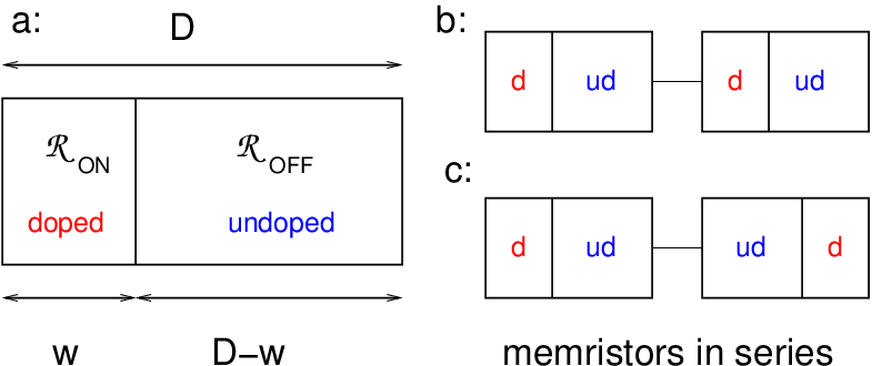
We start this section with the elegant model of a memristor presented in Ref. 10. It consisted of a thin film (5 nm thick) with one layer of insulating TiO2 and oxygen-poor TiO2-x each, sandwiched between platinum contacts. The oxygen vacancies in the second layer behave as charge +2 mobile dopants. These dopants create a doped TiO2 region, whose resistance is significantly lower than the resistance of the undoped region. The boundary between the doped and undoped regions, and therefore the effective resistance of the thin film, depends on the position of these dopants. It, in turn, is determined by their mobility ( cm2/V.s) [10] and the electric field across the doped region. [11] Figure 2 shows a schematic of a memristor of size ( 10 nm) modeled as two resistors in series, the doped region with size and the undoped region with size . The effective resistance of such a device is
| (1) |
where (1k) [10] is the resistance of the memristor if it is completely doped, and is its resistance if it is undoped. Although Eq.(1) is valid for arbitrary values of and , experimentally, the resistance of the doped TiO2 film is significantly smaller than the undoped film, and therefore . In the presence of a voltage the current in the memristor is determined by Kirchoff’s voltage law . The memristive behavior of this system is reflected in the time-dependence of size of the doped region . In the simplest model - the linear-drift model - the boundary between the doped and the undoped regions drifts at a constant speed given by
| (2) |
where we have used the fact that a current corresponds to a uniform electric field across the doped region. Since the (oxygen vacancy) dopant drift can either expand or contract the doped region, we characterize the “polarity” of a memristor by , where corresponds to the expansion of the doped region. We note that “switching the memristor polarity” means reversing the battery terminals, or the plates of a capacitor (in an MC circuit) or reversing the direction of the initial current (in an ML circuit). Eqns.(1)-(2) are used to determine the i-v characteristics of a memristor. Integrating Eq.(2) gives
| (3) |
where is the initial size of the doped region. Thus, the width of the doped region changes linearly with the amount of charge that has passed through it. [12] is the charge that is required to pass through the memristor for the dopant boundary to move through distance (typical parameters [10] imply C). It provides the natural scale for charge in a memristive circuit. Substituting this result in Eq.(1) gives
| (4) |
where is the effective resistance (memristance) at time . Eq.(4) shows explicitly that the memristance depends purely on the charge that has passed through it. Combined with , Eq.(4) implies that the model presented here is an ideal memristor. (We recall that is equivalent to ). The prefactor of the -dependent term is proportional to and becomes increasingly important when is small. In addition, for a given , the memristive effects become important only when . Now that we have discussed the memristor model from Ref. 10, in the following paragraphs we obtain analytical results for its i-v characteristics.
For an ideal circuit with a single memristor and a voltage supply, Kirchoff’s voltage law implies
| (5) |
The solution of this equation, subject to the boundary condition is
| (6) | |||||
| (7) |
where is the magnetic flux associated with the voltage . Eqs.(6)-(7) provide analytical results for i-v characteristics of an ideal memristor circuit. Eq.(6) shows that the charge is an invertible function of the magnetic flux [3, 4] consistent with the defining equation . Eq.(7) shows that a memristor does not introduce a phase-shift between the current and the voltage, if and only if . Therefore, unlike an ideal capacitor or an inductor, is a purely dissipative element. [3] For an AC voltage , the magnetic flux is . Note that although , . Therefore, it follows from Eq.(7) that the current will be a multi-valued function of the voltage . It also follows that since , the memristive behavior is dominant only at low frequencies . Here is the time that the dopants need to travel distance under a constant voltage . and provide the natural time and frequency scales for a memristive circuit (typical parameters [10] imply ms and KHz). We emphasize that Eq.(6) is based on the linear-drift model, Eq.(2), and is valid [12] only when the charge flowing through the memristor is less than when or when . It is easy to obtain a diversity of i-v characteristics using Eqns.(6) and (7), including those presented in Ref. 10 by choosing appropriate functional forms of . Figure 3 shows the theoretical i-v curves for for (red solid), (green dashed), and (blue dotted). In each case, the high initial resistance leads to the small slope of the i-v curves at the beginning. For as the voltage increases, the size of the doped region increases and the memristance decreases. Therefore, the slope of the i-v curve on the return sweep is large creating a hysteresis loop. The size of this loop varies inversely with the frequency . At high frequencies, , the size of the doped region barely changes before the applied voltage begins the return sweep. Hence the memristance remains essentially unchanged and the hysteretic behavior is suppressed. The inset in Fig. 3 shows the theoretical q- curve for that follows from Eq.(6).
Thus, a single memristor shows a wide variety of i-v characteristics based on the frequency of the applied voltage. Since the mobility of the (oxygen vacancy) dopants is low, memristive effects are appreciable only when the memristor size is nano-scale. Now, we consider an ideal circuit with two memristors in series (Fig. 2). It follows from Kirchoff’s laws that if two memristors and have the same polarity, , they add like regular resistors, whereas when they have opposite polarities, , the -dependent component is suppressed, . The fact that memristors with same polarities add in series leads to the possibility of a superlattice of memristors with micron dimensions instead of the nanoscale dimensions. We emphasize that a single memristor cannot be scaled up without losing the memristive effect because the relative change in the size of the doped region decreases with scaling. A superlattice of nano-scale memristors, on the other hand, will show the same memristive effect when scaled up. We leave the problem of two memristors in parallel to the Reader.
These non-trivial properties of an ideal memristor circuit raise the following question: What are the properties of basic circuits with a memristor and a capacitor or an inductor? (A memristor-resistor circuit is trivial.) We will explore this question in the subsequent sections.
III Ideal MC and ML Circuits
Let us consider an ideal MC circuit with a capacitor having an initial charge and no voltage source. The effective resistance of the memristor is determined by its polarity (whether the doped region increases or decreases), and since the charge decay time-constant of the MC circuit depends on its effective resistance, the capacitor discharge will depend on the memristor polarity. Kirchoff’s voltage law applied to an ideal MC circuit gives
| (8) |
where is the charge on the capacitor. We emphasize that the -dependence of the memristance here is because if is the remaining charge on the capacitor, then the charge that has passed through the memristor is (). Eq.(8) is integrated by rewriting it as where and . We obtain the following implicit equation
| (9) |
where is the memristance when the entire charge has passed through the memristor. [12] A small -expansion of Eq.(9) shows that the initial current is independent of the memristor polarity , and the large- expansion shows that the charge on the capacitor decays exponentially, . In the intermediate region, the naive expectation is not the self-consistent solution of Eq.(9). Therefore, although a memristor can be thought of as an effective resistor, its effect in an MC circuit is not captured by merely substituting its time-dependent value in place of the resistance in an ideal RC circuit. Qualitatively, since the memristance decreases or increases depending on its polarity, we expect that when the MC circuit will discharge faster than an RC circuit with same resistance . That RC circuit, in turn, will discharge faster than the same MC circuit when . Figure 4 shows the theoretical q-t curves obtained by (numerically) integrating Eq.(8). These results indeed fulfill our expectations. We note that Eq.(9), obtained using the linear-drift model, is valid for when which guarantees that the final memristance is always positive. [12] The inset in Fig. 4 shows the time-evolution of the size of the doped region obtained using Eq.(3) and confirms the applicability of the linear-drift model. We remind the Reader that changing the polarity of the memristor can be accomplished by exchanging the plates of the fully charged capacitor.
It is now straightforward to understand an ideal MC circuit with a direct-current (DC) voltage source and an uncharged capacitor. This problem is the time-reversed version of an MC circuit with the capacitor charge and no voltage source. The only salient difference is that in the present case, the charge passing through the memristor is the same as the charge on the capacitor. Using Kirchoff’s voltage law we obtain the following implicit result,
| (10) |
where is the memristance when . As before, Eq.(10) shows that when , the ideal MC circuit charges faster (slower) than an ideal RC circuit with the same resistance . In particular, the capacitor charging time for (the doped region widens and the memristance reduces with time) decreases steeply as the DC voltage , the maximum voltage at which the linear-drift model is applicable. [12]
Now we turn our attention to an ML circuit. Ideal RC and RL circuits are described by the same differential equation () with same boundary conditions. Therefore they have identical solutions [2] and . As we will see below, this equivalence breaks down for MC and ML circuits. Let us consider an ideal ML circuit with initial current . Kirchoff’s voltage law implies that
| (11) |
The solution of this equation above is given by where , , and are the two real roots of . We integrate the implicit result using partial fractions and get
| (12) |
where is characteristic time associated with the ML circuit. The current in the circuit is
| (13) |
Eqs.(12)-(13) provide the set of analytical results for an ideal ML circuit. At small- Eq.(13) becomes , whereas the large- expansion shows that the current decays exponentially, . Since depends on the polarity of the memristor, , the ML circuit with discharges slower than its RL counterpart whereas the same ML circuit with discharges faster than the RL counterpart. Figure 5 shows the theoretical i-t curves for an ML circuit obtained from Eq.(13); these results are consistent with our qualitative analysis. Note that the net charge passing through the memristor in an ML circuit is . Therefore an upper limit on initial current for the validity of the linear-drift model [12] is given by (). As in the case of an ideal MC circuit charge, the ML circuit current decays steeply as approaches this upper limit.
Figs. 4 and 5 suggest that ideal MC and ML circuits have a one-to-one correspondence analogous to the ideal RC and RL circuits. Therefore, it is tempting to think that solution of an ideal ML circuit with a DC voltage is straightforward. (In a corresponding RL circuit, the current asymptotically approaches for ). The relevant differential equation obtained using Kirchoff’s voltage law,
| (14) |
shows that it is not the case. In an ML circuit, as the current asymptotically approaches its maximum value, it can pump an arbitrarily large charge through the memristor. Hence, for any non-zero voltage, no matter how small, the linear-drift model breaks down at large times when exceeds () or becomes negative (). This failure of the linear-drift model reflects the fact that when the (oxygen vacancy) dopants approach either end of the memristor, their drift is strongly suppressed by a non-uniform electric field. Thus, unlike the ideal RL circuit, the steady-state current in an ideal ML circuit is not solely determined by the resistance but also by the inductor. In the following section, we present more realistic models of the dopant drift that take into account its suppression near the memristor boundaries.
IV Models of Non-linear Dopant Drift
The linear-drift model used in preceding sections captures the majority of salient features of a memristor. It makes the ideal memristor, MC, and ML circuits analytically tractable and leads to closed-form results such as Eqs. (7), (9), and (13). We leave it as an exercise for the Reader to verify that these results reduce to their well-known R, RC, and RL counterparts in the limit when the memristive effects are negligible, . The linear drift model suffers from one serious drawback: it does not take into account the boundary effects. Qualitatively, the boundary between the doped and undoped regions moves with speed in the bulk of the memristor, but that speed is strongly suppressed when it approaches either edge, or . We modify Eq.(2) to reflect this suppression as follows [10]
| (15) |
The window function satisfies to ensure no drift at the boundaries. The function is symmetric about and monotonically increasing over the interval , . These properties guarantee that the difference between this model and the linear-drift model, Eq.(2), vanishes in the bulk of the memristor as . Motivated by this physical picture, we consider a family of window functions parameterized by a positive integer , . Note that satisfies all the constraints for any . The equation has 2 real roots at , and complex roots that occur in conjugate pairs. As increases is approximately constant over an increasing interval around and as , for all except at . (For example, only for and .) Thus, with large provides an excellent non-linear generalization of the linear-drift model without suffering from its limitations. We note that at finite Eq.(15) describes a memristive system [4, 10] that is equivalent to an ideal memristor [3, 10] when or when the linear-drift approximation is applicable. It is instructive to compare the results for large with those for , , when the window function imposes a non-linear drift over the entire region . [10] For it is possible to integrate Eq.(15) analytically and we obtain
| (16) |
As expected, when the suppression at the boundaries is taken into account, the size of the doped region satisfies for all and asymptotically approaches when . For , we numerically solve Eq.(15) with Kirchoff’s voltage law applied to an ideal MCL circuit
| (17) |
using the following simple algorithm
| (18) | |||||
| (19) | |||||
| (20) |
Here, is the discrete time-step and and stand for the doped-region width, current, and charge at time respectively. The algorithm is stable and accurate for small .
Figure 6 compares the theoretical i-v results for a single memristor with two models for the dopant drift: a model with non-uniform drift over the entire memristor (red solid) and a model in which the dopant drift is heavily suppressed only near the boundaries (green dashed). We see that as increases, beyond a critical voltage the memristance drops rapidly to as the entire memristor is doped. Figure 7 shows theoretical results for a discharging ideal MC circuit obtained using two models: one with (green dashed for and blue dash-dotted for ) and the other with (red solid for and magenta dotted for ). The corresponding window functions are shown in the inset. We observe that the memristive behavior is enhanced as increases, leading to a dramatic difference between the decay times of a single MC circuit when (red solid) and (magenta dotted). Fig. 7 also shows that fitting the experimental data to these theoretical results can determine the window function that best captures the realistic dopant drift for a given sample.
V Oscillations and damping in an MCL Circuit
In this section, we discuss the last remaining elementary circuit, namely an ideal MCL circuit. First let us recall the results for an ideal RCL circuit. [1] For a circuit with no voltage source and an initial charge , the time-dependent charge on the capacitor is given by
where defines an underdamped circuit and defines an overdamped circuit. The two results are continuous at (critically damped circuit). Thus, an RCL circuit is tuned through the critical damping when the resistance in the circuit is increased beyond .
The non-linear differential equation describing an MCL circuit, Eq.(17), cannot be solved analytically due to the -dependent memristance. Figure 8 shows theoretical q-t curves for a single MCL circuit obtained by numerically integrating Eqs.(15) and (17) using window function. When (red solid) the circuit is underdamped because as the capacitor discharges the memristance reduces from its initial value . When (dashed green), the discharging capacitor increases the memristance. Therefore, when the MCL circuit is overdamped. For comparison the blue dotted line shows the theoretical q-t result for an ideal RCL circuit with resistance that is chosen such that the circuit is close to critically damped, . Fig. 8 implies that if we exchange the plates of the capacitor in an MCL circuit, the charge will decays rapidly or oscillate. This property is unique to an MCL circuit and arises essentially due to the memristive effects.
For completeness, we briefly discuss the behavior of an MCL circuit driven by an AC voltage source , with zero initial charge on the capacitor. For an ideal RCL circuit, the steady-state charge oscillates with the driving frequency and amplitude . For a given circuit, the maximum amplitude occurs at resonance, and diverges as . [1] Fig. 9 shows theoretical q-t curves for an ideal MCL circuit with driven with . The red solid line corresponds to low LC frequency , the dashed green line corresponds to resonance, , and the dotted blue line corresponds to high LC frequency . We find that irrespective of the memristor polarity, the memristive effects are manifest only in the transient region. We leave it as an exercise for the Reader to explore the strong transient response for and compare it with the steady state response at resonance .
VI Discussion
In this tutorial, we have presented theoretical properties of the fourth ideal circuit element, the memristor, and of basic circuits that include a memristor. In keeping with the revered tradition in physics, the existence of an ideal memristor was predicted in 1971 [3] based purely on symmetry argument [13]; however, its experimental discovery [6, 7, 8, 9, 10] and the accompanying elegant physical picture [10, 15] took another 37 years. The circuits we discussed complement the standard RC, RL, LC, RCL circuits, thus covering all possible circuits that can be formed using the four ideal elements (a memristor, a resistor, a capacitor, and an inductor) and a voltage source. We have shown in this tutorial that many phenomena - the change in the discharge rate of a capacitor when the plates are switched or change in the current in a circuit when the battery terminals are swapped - are attributable to a memristive component in the circuit. [14, 15] In such cases, a real-world circuit can only be mapped on to one of the ideal circuits with memristors.
The primary property of the memristor is the memory of the charge that has passed through it, reflected in its effective resistance . Although the microscopic mechanisms for this memory can be different, [10, 15] dimensional analysis implies that the memristor size and mobility provide a unit of magnetic flux that characterizes the memristor. Although the underlying idea behind a memristor is straightforward, its nano-scale size remains the main challenge in creating and experimentally investigating basic electrical circuits discussed in this article.
We conclude this tutorial by mentioning an alternate possibility. It is well-known that an RCL circuit is equivalent [1] to a 1-dimensional mass+spring system in which the position of the point mass is equivalent to the charge , the mass is , the spring constant is , and the viscous drag force is given by where . Therefore, a memristor is equivalent to a viscous force with a -dependent drag coefficient, . Choosing , where is the typical stretch of the spring, will create the equivalent of an MCL circuit.Since a viscous force naturally occurs in fluids, a vertical mass+spring system in which the mass moves inside a fluid with a large vertical viscosity gradient can provide a macroscopic realization of the MCL circuit.
Acknowledgements.
It is a pleasure to thank R. Decca, A. Gavrin, G. Novak, and K. Vasavada for helpful discussions and comments. This work was supported by the IUPUI Undergraduate Research Opportunity Program (UROP). S.J.W. acknowledges a UROP Summer Fellowship.References
- [1] See, for example, J. Walker, Fundamentals of Physics (John Wiley & Sons Inc., New York), 8th ed.; H.D. Young and R.A. Freedman, University Physics (Addison Wesley, New York), 12th ed.; P.A. Tipler and G. Mosca, Physics for Scientists and Engineers (W.H. Freeman and Company, New York), 6th ed.; H.C. Ohanian and J.T. Markert, Physics for Engineers and Scientists (W.W. Norton and Company, New York), 3rd ed.
- [2] R.P. Feynman, R.B. Leighton, and M. Sands, The Feynman Lectures on Physics, vol. II (Addison Wesley, New York).
- [3] L.O. Chua, “Memristor - the missing circuit element,” IEEE Trans. Circuit Theory 18, 507-519 (1971).
- [4] L.O. Chua and S.M. Kang, “Memristive devices and systems,” Proc. IEEE 64, 209-223 (1976).
- [5] L.O. Chua, “Device modeling via non-linear circuit elements,” IEEE Trans. Circuits and Systems 27, 1014-1044 (1980).
- [6] Over last two decades, devices with programmable variable resistance, also called memristors, have been fabricated. [7, 8, 9] They show hysteretic i-v characteristics, but do not discuss the defining property of a memristor, the invertible relationship between the charge and the magnetic flux. The interplay between electronic and ionic transport in these samples is non-trivial, and none of them have presented a simple physical picture similar to the one in Ref. 10.
- [7] S. Thakoor, A. Moopenn, T. Daud, and A.P. Thakoor, “Solid-state thin film memristor for electronic neural networks,” J. Appl. Phys. 67, 3132-3135 (1990).
- [8] V.V. Erokhin, T.S. Berzina, and M.P. Fontana, “Hybrid electronic device based on polyaniline-polyethyleneoxide junction,” J. Appl. Phys. 97, 064501 (2005).
- [9] V. Erokhin, T.S. Berzina, and M.P. Fontana, “Polymeric elements for adaptive networks,” Cryst. Report 52, 159-166 (2007).
- [10] D.B. Strukov, G.S. Snider, D.R. Stewart, and R.S. Williams, “The missing memristor found,” Nature (London) 453, 80-83 (2008); J.M. Tour and T. He, “The fourth element,” ibid 42-43 (2008).
- [11] For an introduction to semiconductors, see chapter 42, and mobility, see chapter 25, H.D. Young and R.A. Freedman, University Physics (Addison Wesley, New York), 12th ed.
- [12] The linear-drift model is valid only when for all . This constraint provides limits on the flux , the initial capacitor charge or the DC voltage , and the initial current . We compare linear and non-linear dopant drift models in Sec. IV.
- [13] The displacement-current in Maxwell’s equations, a positron, and a magnetic monopole are a few historical examples. The first two have been experimentally observed, while the third one remains elusive.
- [14] F. Miao, D. Ohlberg, D.R. Stewart, R.S. Williams, and C.N. Lau, “Quantum conductance oscillations in Metal/Molecule/Metal switches at room temperature,” Phys. Rev. Lett. 101, 016802 (2008).
- [15] Y.V. Pershin and M.Di Ventra, “Spin memristive systems,” arXiv:0806.2151.
Figures