Excited-state spectroscopy on a quantum dot side-coupled to a quantum wire
Abstract
We report excited-state spectroscopy on a quantum dot side-coupled to a quantum wire with accurate energy estimation. Our method utilizes periodic voltage pulses on the dot, and the energy calibration is performed with reference to the bias voltage across the wire. We demonstrate the observation of the orbital excited state and the Zeeman splitting in a single dot.
Semiconductor quantum dots are promising candidates for quantum bits (qubits) [1]. In a conventional dot with two leads, the current through the dot as a function of the source-drain bias and a gate voltage provides the information of the excited states as well as the ground states [2]. However in the application to quantum information processing, the number of leads is desired to be as small as possible, because the connection to the outside circuits brings in quantum decoherence. Besides the decoherence, a dot with a single-lead has a number of advantages such as the spatial compactness, the easiness to go down to the few electron regime [3], and so on.
In single-lead dots, the spectroscopic information is usually given through the interference (the Fano effect) [5, 4] or the charge detection [6]. However, these measurements were limited to the spectroscopy of the ground states. To overcome the difficulty, a method combining remote charge sensing and pulsed electrostatic gating was demonstrated for excited-state spectroscopy on a nearly closed quantum dot [7]. Now the remaining difficulty is to find out a “measure” for the energy, in other words the conversion factor from the gate voltage to the energy, without applying finite voltage nor current across the dots. So far such conversion is performed by changing the effective dot configuration with gate voltages or by numerical simulation. The former inevitably causes significant variation in the electrostatic parameters, while the latter just gives approximate estimation. In order to make precise meaningful spectroscopy, a method to obtain the reliable conversion factor is indispensable.
In this letter, we show that the conversion factor can be precisely obtained in a specially designed single-lead dot, namely a quantum dot side-coupled to a quantum wire. Our method is based on the one by Elzerman et al. [7], but differs in that the bias voltage can be applied across the quantum wire. When the wire length is much shorter than the mean free path, the bias on the wire creates two quasi-Fermi levels [8, 9]. If the dot can detect the non-equilibrium energy distribution on the gate voltage axis, this gives the conversion factor. It is demonstrated that the present method can be applied to the measurement of spin-splittings as well as orbital excited states.
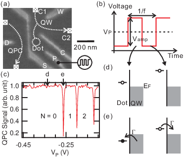
Figure 1(a) shows a scanning electron micrograph of our device fabricated on a GaAs/AlGaAs heterostructure containing a 2DEG 60 nm below the surface. Applying negative voltages on gates S, P, C and W, we prepare a quantum dot which couples to a short quantum wire (QW in the figure). A quantum point contact (QPC), formed between gates S and D, is used for remote charge sensing [6]. The potential barrier due to gate S is set high enough so that no exchange of electrons occurs between QPC and the dot.
First we describe the experiments at zero bias voltage. A train of voltage pulses is applied on the plunger gate P. The pulse train is a rectangular wave with duty ratio 0.5, and is characterized by amplitude , repetition frequency and center voltage [Fig. 1(b)]. The synchronized current oscillation in QPC is lock-in detected.
The voltage pulses applied on gate P shift the energy levels in the dot up and down. If an energy level of the dot is always above the Fermi level of QW , the level is always empty and cannot exchange electrons with QW [Fig. 1(d)]. The signal in this case reflects the direct capacitive coupling between gate P and QPC. When is shifted and gets into the region where the level is swinging, and if is low enough, the dot captures and emits an electron in phase with the pulse [Fig. 1(e)]. The captured electron compensates the effect of the pulsed voltage on gate P, thus the current oscillation through QPC becomes smaller.
Figure 1(c) shows a typical signal of QPC as a function of (the coupling gate voltage V, mV and Hz), in which three dips are observed. Here, we operate in the regime where tunneling time between the wire and the dot is sufficiently shorter than the pulse duration and the charge-up of the dot completely follows the pulses. For V, dips are no longer observed, indicating full depletion of electrons in the dot.

The following experiments are carried out around a dip between zero- and one-electron states. and are optimized for making comparable with . The QPC signal at V, mV and Hz is shown in Fig. 2(a). The electron response produces a hollow in V. This corresponds to an “energy window”, within which the electrons can go to and from the dot. The hollow is deeper in the less negative side (region c).
This two-step structure is a hallmark of the presence of the excited state and interpreted as follows. Because , the charging of the dot stochastically follows the pulses. In region b, movement of electrons occurs only via the ground state [Fig. 2(b)]. When the total voltage on gate P is , only the ground state is below and can accept an electron from QW with tunneling rate . On the other hand, in region c, an electron can flow into both the ground and excited states [Fig. 2(c)]. This makes effective tunneling rate larger than and the signals take smaller values, where is the tunneling rate of the excited state. Since the measurement is performed in zero-magnetic field and one-electron state, the excited state is attributed to orbital one. Note that simultaneous occupation with two electrons is prohibited by the charging energy and the change in the QPC signal is solely due to that in .
Figure 2(d) shows the QPC signal as a function of and . For clarity, we subtracted the background that comes from the direct coupling to gate P. As expected, the width of the hollow region agrees with . The deeper hollow region appears around mV. When the excited state is accessible, the width of the shallow region is constant against , and denoted as in the figure. reflects the energy difference between the ground and the first excited orbital states . The two quantities are connected by a conversion factor ().

Next, to estimate the value of , we apply finite bias voltage on contact C1, and contact C2 is grounded. Since the mean free path of the electrons is about m, and is much longer than QW, the energy relaxation in QW is negligible. This produces non-equilibrium energy distribution inside QW, as illustrated in Fig. 3(a) [8, 9]. There are two quasi-Fermi levels and , which correspond to C1 and C2 respectively. Now the dot couples to these two kinds of electrons and produces signals for exchanging the electrons with them. The condition of is adjusted so that only the ground state may be in the energy window. Hence, two dips due to and are expected in the QPC signal.
Figure 3(b) shows the QPC signal with changing from -1 mV (bottom) to 1 mV (top). We in fact observe two types of dips, one of which shifts the position with , while the other is fixed around V. The former corresponds to . The relation between the dip position and shows excellent linearity. We obtain by linear fitting [Fig. 3(c)]. Here, the contribution from series resistance, which is estimated from the resistance when we remove the confinement of QW, has also been subtracted. With this procedure, we obtain the value eV/V. Then the energy difference between the ground and excited orbitals is given as 2.3 meV. We would like to emphasize that this calibration can be performed without changing any relevant parameter of the side-coupled system.
In Fig. 3(b), the shifting dips have higher visibility, reflecting the difference in the coupling between the dot and the two quasi-Fermi levels. In our device, the entrance of the dot is directed to C1 [Fig. 1(a)]. This asymmetry would make stronger coupling between C1 and the dot. This is further confirmed by grounding C1 and sweeping the voltage of C2. As shown in Fig. 3(d), the clearer dips for C1 are fixed and the others shift with the bias on C2. These also support the picture that the two quasi-Fermi levels are formed and the dot couples to them.

For further checking the validity of our method, we now apply it to the Zeeman splitting. Magnetic fields lift the spin degeneracy and produce the Zeeman splitting , where is the g-factor and is the Bohr magneton. It has been reported that the g-factor in heterostructure is smaller than the bulk value of in GaAs [10, 11, 12, 13]. We apply in-plane magnetic fields in order to minimize the magnetic effect on orbital states of the dot. The QPC signal as a function of and at 14 T is shown in Fig. 4(a). Here, the range of is limited so that the orbital excited state is not visible. The background is again subtracted to improve visibility. The two-step hollow structure similar to Fig. 2(d) is observed. In this case, the excited state is due to lifting of the Kramers degeneracy by magnetic field and the width of the shallow region reflects . By calibrating the conversion factor at each field, we obtain as a function of magnetic field, which is shown in Fig. 4(b). Though the signal-to-noise ratio was not high enough to resolve the Zeeman splitting at lower fields, the data at high fields align along a line pointing the origin as shown in Fig. 4(b). The gradient gives in agreement with previous reports on transport measurements [11, 12, 13], certifying the validity and the effectiveness of the present method.
In this work, we demonstrate excited-state spectroscopy on a side-coupled quantum dot with accurate energy estimation by utilizing voltage pulse on the dot and energy calibration with bias voltage over the wire. The orbital excited state as well as the Zeeman splitting are detected with this method and the obtained g-factor in the dot is in good agreement with the measurements so far reported.
We thank Y. Hashimoto and S. Tamiya for technical supports. This work is supported by Grant-in-Aid for Scientific Research and Special Coordination Funds for Promoting Science and Technology.
References
- [1] D. Loss and D. P. DiVincenzo, Phys. Rev. A 57, 120 (1998).
- [2] L. P. Kouwenhoven, T. H. Oosterkamp, M. W. Danoesastro, M. Eto, D. G. Austing, T. Honda, and S. Tarucha, Science 278, 1788 (1997).
- [3] T. Otsuka, E. Abe, S. Katsumoto, Y. Iye, G. L. Khym, and K. Kang, J. Phys. Soc. Jpn. 76, 084706 (2007).
- [4] A. C. Johnson, C. M. Marcus, M. P. Hanson, and A. C. Gossard, Phys. Rev. Lett. 93, 106803 (2004).
- [5] K. Kobayashi, H. Aikawa, A. Sano, S. Katsumoto, and Y. Iye, Phys. Rev. B 70, 035319 (2004).
- [6] M. Field, C. G. Smith, M. Pepper, D. A. Ritchie, J. E. F. Frost, G. A. C. Jones, and D. G. Hasko, Phys. Rev. Lett. 70, 1311 (1993).
- [7] J. M. Elzerman, R. Hanson, L. H. W. van Beveren, L. M. K. Vandersypen, and L. P. Kouwenhoven, Appl. Phys. Lett. 84, 4617 (2004).
- [8] H. Pothier, S. Guéon, N. O. Birge, D. Esteve, and M. H. Devoret, Phys. Rev. Lett. 79, 3490 (1997).
- [9] S. De Franceschi, R. Hanson, W. G. van der Wiel, J. M. Elzerman, J. J. Wijpkema, T. Fujisawa, S. Tarucha, and L. P. Kouwenhoven, Phys. Rev. Lett. 89, 156801 (2002).
- [10] M. Dobers, K. von Klitzing, and G. Weimann, Phys. Rev. B 38, 5453 (1988).
- [11] R. M. Potok, J. A. Folk, C. M. Marcus, V. Umansky, M. Hanson, and A. C. Gossard, Phys. Rev. Lett. 91, 016802 (2003).
- [12] R. Hanson, B. Witkamp, L. M. K. Vandersypen, L. H. W. van Beveren, J. M. Elzerman, and L. P. Kouwenhoven, Phys. Rev. Lett. 91, 196802 (2003).
- [13] L. H. W. van Beveren, R. Hanson, I. T. Vink, F. H. L. Koppens, L. P. Kouwenhoven, and L. M. K. Vandersypen, New J. Phys. 7, 182 (2005).