Abstract
The physics of the phase shift in ferromagnetic Josephson junctions enables a range of applications for spin-electronic devices and quantum computing. In this respect our research is devoted to the evaluation of the best materials for the development and the realization of the quantum devices based on superconductors and at the same point towards the reduction of the size of the employed heterostructures towards and below nano-scale. In this chapter we report our investigation of transitions from 0 to states in Nb Josephson junctions with strongly ferromagnetic barriers of Co, Ni, Ni80Fe20 (Py) and Fe. We show that it is possible to fabricate nanostructured Nb/ Ni(Co, Py, Fe)/Nb -junctions with a nano-scale magnetic dead layer and with a high level of control over the ferromagnetic barrier thickness variation. In agreement with the theoretical model we estimate, from the oscillations of the critical current as function of the ferromagnetic barrier thickness, the exchange energy of the ferromagnetic material and we obtain that it is close to bulk ferromagnetic materials implying that the ferromagnet is clean and S/F roughness is minimal. We conclude that S/F/S Josephson junctions are viable structures in the development of superconductor-based quantum electronic devices; in particular Nb/Co/Nb and Nb/Fe/Nb multilayers with their low value of the magnetic dead layer and high value of the exchange energy can readily be used in controllable two-level quantum information systems. In this respect, we discuss applications of our nano-junctions to engineering magnetoresistive devices such as programmable pseudo-spin-valve Josephson structures.
1 Introduction
Conventional electronics is based on the transport of electrical charge carriers, however the necessity to have more versatile and efficient devices on micro- and nano-scale has diverted the attention towards the spin of the electron rather than its charge: this is the essence of spintronics. Although spintronic devices were traditionally built with semiconductors and/or ferromagnetic materials, nowadays hybrid structures constituted by superconductors (S) and ferromagnetic (F) materials are emerging as promising alternatives. They serve as candidates to realize and investigate systems useful both as testgrounds to probe fundamental physics questions, and as realistic elements for application in the spintronics industry thanks to the improved degree of control on the spin polarized current.
In hybrid S/F structures it has been verified that, due to the simultaneous presence of these two competitive orders, peculiar effects appear: the superconductivity is reduced by the spin polarization of the F layer, while due to the proximity effect the Cooper pairs can enter in the superconductor resulting in a oscillatory behavior of the density of states. The last effect opens the doors towards new and exciting developments for the realization of quantum electronic devices. In fact in S/F/S systems, due to the oscillations of the order parameter, some oscillations manifest in the Josephson critical current as a function of the ferromagnetic barrier thickness evidencing the presence of two different states, 0 and , corresponding to the sign change of the Josephson critical current.
Our research, presented in this chapter, fits in this rapidly developing and exciting area of condensed matter physics [1]. Within the context of the spin polarized devices based on the interplay between superconductivity and ferromagnetism, we have fabricated S/F/S nano-structured Josephson junctions constituted by a low temperature superconductor, Niobium (Nb), and strong ferromagnetic metal, Nickel(Ni), Ni80Fe20 (Py), Cobalt (Co) and Iron (Fe), and we have investigated their magnetic and electrical properties. These structures have evidenced a small magnetic dead layer and oscillations of the critical current as a function of the ferromagnetic barrier. These oscillations show excellent fits to existing theoretical models. We also determine the Curie temperature for Ni, Py and Co. In the case of Co and Fe we estimate the mean free path to confirm that the oscillations are in the clean limit and from the temperature dependence of the product we show that its decay rate exhibits a nonmonotonic oscillatory behavior with the ferromagnetic barrier thickness. We investigate the presence of the Shapiro steps on the vs curve applying a microwave and the effect of the magnetic field on the maximum supercurrent. In this last case we find oscillations of the maximum of the supercurrent corrisponding to a Fraunhofer pattern. Finally, in the case of Co barrier, focusing in detail on a single 0- phase transition we show evidence for the appearance of a second harmonic in the current-phase relation at the minimum of the critical current. For the high value of the exchange energies and small magnetic dead layer the S/F/S structures with Co or Fe barrier can be considered as good candidates for the realization of quantum devices.
2 F/S Junctions: Basic Aspects
The aim of this section is to give an outline of the physics of the Ferromagnetic-Superconducting (F/S) interfaces (for a review see [2]).

Andreev reflection plays an important role to understand the transport process in F/S junctions. The Andreev reflection near the Fermi level preserves energy and momentum but does not preserve spin, in other words the incoming electron and the reflected hole have opposite spin. This is irrelevant for the transport in N/S junctions (N stands for normal metal) due to the spin-rotation symmetry. On the other hand at F/S interfaces, since the spin-up and spin-down bands in F are different, the spin flipping changes the conductance profile. In particular in fully spin-polarized metals all carriers have the same spin and the Andreev reflection is totaly suppressed; therefore, at zero bias voltage the normalized conductance becomes zero (see Fig. 1). In general, for arbitrary polarization , it can easily be shown that
| (1) |
where, in terms of the spin-up and spin-down electrons, the spin polarization is defined as
| (2) |
From this analysis it has been shown that the point contact measurements based on the Andreev reflection process give a quantitative estimation of the polarization of the ferromagnetic material [3, 4]. In fact from the reduction of the zero bias conductance peak it is possible with a modified Blonder-Tinkham-Klapwijk model to estimate the polarization .
In a ferromagnet in proximity to a superconductor, the coherence length , due to the presence of the exchange field , is given by:
| (3) |
where is the diffusive coefficient. If the exchange energy is large compared to the temperature, , the coherence length is much shorter than in the case of the N/S proximity effect. In addition to the reduced coherence length compared to typical N/S structures, a second characteristic property arises from the complex nature of the coherence length: the induced pair amplitude oscillates spatially in the ferromagnetic metal as a consequence of the exchange field acting upon the spins of the two electrons forming a Cooper-pair [5, 6, 7, 8] (see Fig. 2). This oscillation includes a change of sign and by using appropriate values for the exchange energy and F-layer thickness, negative coupling can be realized. We refer to the state corresponding to a positive sign of the real part of the order parameter as “-state” and that corresponding to a negative sign of the order parameter as “-state”.

Demler et al. [9] gave a qualitative picture of this oscillatory character. They considered a Cooper pair transported adiabatically across an F/S interface, with its electron momenta aligned with the interface normal direction. The pair entering in the F region decays exponentially on the length scale of the normal metal coherence length. Then the up-spin electron, oriented along the exchange field, decreases its energy by , where is the exchange energy of the F layer. On the other hand, the down-spin electron increases its energy by . To compensate this energy variation, the up-spin electron increases its kinetic energy, while the down-spin electron decreases its kinetic energy. As a result the Cooper pair acquires a center-of-mass momentum , which implies the modulation of the order parameter with period , where is the Fermi velocity.

As a consequence of the oscillations of the order parameter, a similar oscillatory behavior is observed for the density of states. This behavior can be explained by considering the spin effect on the mechanism of Andreev reflections [2].
The process is illustrated in Fig. 3 using the energy-momentum dispersion law of the normal metal: in the case of a N/S interface an incoming electron in a normal metal N with energy lower than the superconducting energy gap from the Fermi level can be reflected into a hole at the N/S interface (Andreev Reflection) [10]. If the normal layer is very thin the density of states in N is close to that of the Cooper pair reservoir. The situation is strongly modified if the normal metal is ferromagnetic. As Andreev reflections invert spin-up into spin-down quasiparticles and vice versa, the total momentum difference includes the spin splitting of the conduction band: . The density of states is modified in a thin layer on the order of . In particular, the interference between the electron and hole wave functions produces an oscillating term in the superconducting density of states with period . This effect has been observed experimentally by Kontos et al. [11]
2.1 Theory of the Josephson -junctions
Due to the spatially oscillating induced pair amplitude in F/S proximity structures it is possible to realize negative coupling of two superconductors across a ferromagnetic weak link (S/F/S Josephson junctions). In this case of negative coupling, the critical current across the junction is reversed when compared to the normal case giving rise to an inverted current-phase relation. Because they are characterized by an intrinsic phase shift of , these junctions are called Josephson -junctions.
One of the manifestations of the phase is a non-monotonic variation of the critical temperature and the critical current, with the variation of the ferromagnetic layer thickness () [2]. Referring to the current-phase relation , for a S/I/S Josephson junction the constant and the minimum energy is obtained for . In the case of a S/F/S Josephson junctions the constant can change its sign from positive to negative indicating the transition from the -state to -state. Physically the changing in sign of is a consequence of a phase change in the electron pair wave function induced in the F layer by the proximity effect. Experimentally, measurements of are insensitive to the sign of hence the absolute value of is measured, so we can reveal a non-monotonic behavior of the critical current as a function of the F layer thickness. The vanishing of critical current marks the transition from to state. The dependence of the critical current on the thickness of the ferromagnetic layer in S/I/F/S junctions has been experimentally investigated by Kontos et al. [12]. The quantitative analysis of the S/F/S junctions is rather complicated, because the ferromagnetic layer can modify the superconductivity at the F/S interface. Then other parameters, such as the boundary transparency, the electron mean free path, the magnetic scattering, etc can affect the critical current. It is outside the purpose of this chapter to derive explicitly the expression of the critical current as a function of the F layer, for the interested reader we refer to this review [2].
The majority of experimental studies have concentrated on weak ferromagnets where , where is the superconducting critical temperature, resulting in multiple oscillations in with temperature and . In the case of strong ferromagnets, where , only oscillations of with , and not with temperature, are observed. In this chapter we will present the study of the oscillations of the critical current as a function of for S/F/S Josephson junctions with strong ferromagnetic barriers.
The generic expression of the critical current as a function of F layer is given by:
| (4) |
where is the thickness of the ferromagnet corresponding to the first minimum and is the first experimental value of ( is the normal state resistance), and and are the two fitting parameters. Eq. 4 ranges in the clean and in the dirty limit. In particular, in clean limit, where L is the mean free path of the F layer, . In this way, known and estimating the Fermi velocity from reported values in literature, one can calculate the exchange energy of the ferromagnetic barrier.
Then, in the case of clean limit the oscillations of vs can be modeled by a simpler theoretical model [13] given by:
| (5) |
where in this case the two fitting parameters are and .
On the other hand, in dirty limit we can model the oscillations [14] by the following formula:
| (6) |
where is the superconducting order parameter, is the Matsubara frequency and is given by where is the transmission coefficient and is an integer number. and where is the angle the momentum vector makes relative to the distance normal to the F/S interface. is given by and is the momentum relaxation time. In this case the fitting parameters are , and the mean free path of the ferromagnetic layer.
3 Josephson Junction Fabrication

To investigate the physics of the ferromagnetic -junctions and their possible applications for spin-electronic devices we have realized and characterized Nb (250 nm thick) / Ferromagnetic layer / Nb (250 nm thick) Josephson junctions. As ferromagnetic layer we have used: Ni, Py, Co and Fe. In the case of Co, Fe and Py their respective thicknesses were varied from - nm while, in the case of Ni, was varied from to nm. To assist processing in a focused ion beam (FIB) microscope, a 20 nm normal metal interlayer of Copper (Cu) was deposited inside the outer Nb electrodes, but 50 nm away from the Fe barrier. We remark that the 20 nm of Cu is a thickness smaller than its coherence length, so it is completely proximitized into the Nb, and it does not affect the transport properties of the Josephson junction. Refer to Fig. 4 for an illustration of our heterostructures [1].

The heterostructures employed in this chapter, have been deposited by d.c. magnetron sputtering. In a single deposition run, multiple silicon substrates were placed on a rotating holder which passed in turn under three magnetrons: Nb, Cu and the ferromagnetic layer (Fe, Co, Py or Ni). The speed of rotation was controlled by a computer operated stepper motor with a precision angle of better than 3.6∘ and each sample was separated by an angle of at least 10∘. Prior to the deposition each target material was calibrated and the deposition rates were estimated with an Atomic Force Microscopy (see table 1 for a summary of the deposition parameters for all target materials presented in this chapter). In the case of the ferromagnetic materials (Co, Py, Fe and Ni) the rates of deposition, and hence , were obtained by varying the speed of each single chip which moves under the ferromagnetic target while maintaining constant power to the magnetron targets and Ar pressure. This was achieved by knowing the chip position relative to the target material () and by programming the rotating flange such that a linear variation of ferromagnetic thickness with , , was achieved. is inversely proportional to the speed of deposition, , and hence it can be shown that in order to achieve a linear variation of one programmes the instantaneous speed, at position and time seconds (i.e. ), of deposition according to
| (7) |
where is the initial speed and is the final speed in units of rpm. This method of varying guaranteed, in all cases, that the interfaces between each layer were prepared under the same conditions while providing precise control of the F layers [15]. Fig. 5 shows an illustration of the sputtering process. For each run, simultaneously, our heterostructures have been deposited on mm2 and mm2 SiO2 substrates. The first ones have been used for the magnetic measurements, the second ones for the realization of Josephson junctions.
| Target material | Rate | Power | Speed range | tF |
|---|---|---|---|---|
| ( at 1 rpm) | (W) | (rpm) | (0.2 nm) | |
| Nb | 6.89 | 90 | .028 | 250 |
| Cu | 4.39 | 30 | 0.22 | 20 |
| Ni | 2.12 | 40 | 0.20-4.2 | 0.5 - 10.5 |
| Co | 1.8 | 40 | 0.36-3.6 | 0.5 - 5.0 |
| Py | 1.64 | 40 | 0.33-3.3 | 0.5 - 5.0 |
| Fe | 2.0 | 40 | 0.22-2.2 | 0.5 -5.0 |
3.1 X-ray Measurements

To confirm our precise control over the ferromagnetic thickness variation we performed low angle X-ray reflectivity of a set of calibration Nb/Co/Nb thin films where the Nb layers had a thickness of nm and the Co barrier thickness was varied from nm to nm [15]. A series of low angle X-ray scans were made and the thickness of the Co layer () was extracted by fitting the period of the Kiessig fringes using a simulation package. It was found that our expected Co barrier thicknesses, , was well correlated with with a mean deviation of 0.2 nm. In the inset of Fig. 6 we show an example of the low angle x-ray data plotted with the equivalent simulation data where was extracted, while in Fig. 6 we report a comparison of with and its deviation.
4 Nanoscale Device Process

We can summarize the realization of the Josephson junctions in three different steps: (i) patterning the films using optical lithography to define the micron scale tracks and the contact pads. Our mask permits etching of at least 14 devices, which allows us to measure numerous devices and to derive good estimates of important parameters, like, for example, characteristic voltage (see Fig. 7 to see an illustration of the mask); (ii) broad beam Ar ion milling ( mAcm-2, V beam) to remove unwanted material from around the mask pattern, thus leaving m tracks for subsequent FIB work; (iii) FIB etching of micron scale tracks to achieve vertical transport [16, 17, 15].
In particular to realize our devices we have used a three-dimensional technique [18]. The wedge holder used in this chapter was designed by D.-J. Kang and it is schematically shown in Fig. 8; it is constituted by three sample lodgings, one in horizontal and two at . Once loaded the sample on the lodging, we can rotate the stage of the FIB at , in this way the beam is perpendicular to the surface of the sample, and the first cut is done; then the sample holder is rotated of around an axis normal to the sample stage, to permit the vertical cut to be done (see Fig. 8). This setup allows to load two samples for each run.

The fabrication procedure is shown in Fig. 9 [19]. A first box with area is milled with pA to realize tracks of about nm (b). The time of milling is about minutes, and this milling can be calibrated using the stage-current/end-point detection measurement. Fig. 10 shows how the milling of different layers can be distinguished, the first peak corresponds to the Nb, the two small peaks correspond to the two Cu layers, and finally the intensity decreases approaching to the SiO2 substrate. The sidewalls of the narrowed track are then cleaned with a beam current of pA. This removes excessive gallium implantation from the larger beam size of the higher beam currents. The cleaning takes - seconds per device. The track width is then nm. The sample is then tilted to , and the two cuts are made with a beam current of pA to give the final device (Fig. 9 (d)) with a device area in the range of m2. This technique permits to achieve vertical transport of the current: in Fig. 9 (e) we show a schematic picture of the current path. In Fig. 11 the final FIB image of a Nb/Cu/Co/Cu/Nb device is presented.


5 Magnetic Measurements
In this section we report magnetic measurements of Nb Josephson junctions with strongly ferromagnetic (F) barriers: Ni, Ni80Fe20 (Py), Co and Fe. From measurements of the magnetization saturation () as a function of the F thickness, our heterostructures have shown a magnetic dead layer ranging between nm and nm. Then we give an estimation of the Curie temperature of the ferromagnetic layer.
5.1 Measurement of the Magnetic Dead Layer
In this section we explain the magnetic properties of Nb-Ni-Nb, Nb-Py-Nb, Nb-Co-Nb and Nb-Fe-Nb heterostructures as a function of F thickness [16, 15, 21, 17].

To this aim we have studied, using a VSM at room temperature, the hysteresis loop of our heterostructures in order to follow the evolution of the magnetization as a function of the applied magnetic field. In Fig. 12 (inset), Fig. 13 (a), 14 (a) and (b), we show a collection of hysteresis loops for different thicknesses of the F barrier. We notice that both the and the width of the hysteresis loop, as expected, decrease with decreasing F layer thickness, and the ferromagnetic order disappears when the F barrier goes to zero. Furthermore from the hysteresis loops we have measured the saturation magnetization as a function of the F barrier to extrapolate the magnetic dead layer.


The presence of a magnetic dead layer has been reported in other studies of S/F/S heterostructures [22, 23, 15] and it can be explained as a loss of magnetic moment of the heterostructures. The magnetic dead layer can be due to numerous factors, as, for example, lattice mismatch at the Nb-F interface resulting in a reduction in the ferromagnetic atomic volume [24] and crystal structure which leads to a reduction in the exchange interaction between neighboring atoms. This loss in exchange interaction manifests itself as a loss in magnetic moment due to a collapse in the regular arrangement of electron spin and magnetic moment and can lead to the suppression in and [25, 26, 27, 28]. Another factor can be the inter-diffusion of the ferromagnetic atoms into the Nb. Like in the case of lattice mismatch this would result in a breakdown of the crystal structure at the interface leading to a reduction in the exchange interaction. The knowledge of the magnetic dead layer is a crucial point within the implementation of -technology, to guarantee the reproducibility and the control of the devices. Extrapolating with a linear fit the saturation magnetization as a function of F thickness, we have obtained the estimation of the magnetic dead layer: nm for Ni (see Fig. 12), nm for Py (see Fig. 13 (b)) and nm for Co (see Fig. 14 (c)).

In the case of Fe the saturation magnetization was measured for three different deposition runs (see Fig. 14 (d)). For each deposition we have obtained similar saturation magnetization and by extrapolating the least-squares fit of these data we have estimated a Fe magnetic dead layer of nm [17]. In Fig. 15 we summarize the magnetic moment vs thickness for Ni, Py, Co and Fe. From these data we can extrapolate the slope of vs . From the theoretical model [29, 30] the predicted slopes are: emu/cm3 for Ni, emu/cm3 for Py, emu/cm3 for Co and emu/cm3 for Fe. On the other hand from our experimental data the slopes of vs for these ferromagnetic materials are suppressed from these expected bulk values: emu/cm3 for Ni, emu/cm3 for Py, emu/cm3 for Co and emu/cm3 for Fe. We can argue that, in our case, we are not considering bulk materials, as reported from Slater and Pauling [29, 30], instead our systems are constituted by F/S sandwiches, so the presence of a superconducting layer, Nb, can induce a weakening of the ferromagnetic properties of the F layer and a possible diffusion of the Nb into the F barrier.
5.2 Calculation of the Curie temperature

We have measured the thermal variation of the saturation magnetization, , of Co, Ni, and Py when sandwiched between thick Nb layers [15]. To be certain, with temperature was not weakened by a thermally activated diffusion of ferromagnetic atoms into Nb, or vice versa; at the interface we measured both the magnetization when warming and cooling. The warming and cooling data agreed for all three barrier systems up to a temperature of 620 K. Above this temperature, was found to drop by virtue of thermally activated diffusion. We have modeled the warming and cooling data of with the following formula
where is the saturation magnetization at absolute 0 K, is the measuring temperature, and and are fitting parameters. This gives values of 1200 K for Co, 571 K for Ni, and 800 K for Py (see Fig.16) in agreement with the bulk values. Data for Ni are the most reliable because we have a full data set. However, in any case these measurements provide that, in our metallic systems, interdiffusion at the ferromagnetic surface cannot be ruled out because the ferromagnetic layer is known to form a variety of magnetic and nonmagnetic alloys with Nb.
6 Transport Measurements
In this section we present the vs curves for the Nb/F/Nb Josephson junctions varying the thickness of the F barrier. All these materials show multiple oscillations of the Josephson critical current with barrier thickness implying repeated - phase-transitions in the superconducting order parameter. The critical current oscillations have been modeled with the clean and dirty limit theoretical models, from this analysis we have extrapolated the exchange energy and the Fermi velocity of the ferromagnetic barrier.
6.1 Experimental Data: Critical Current Oscillations
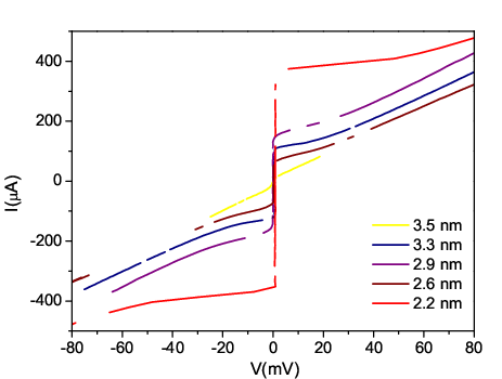
For several junctions on each chip we have measured the current versus voltage from which the critical current () and the normal resistance () of the Josephson junction have been extrapolated. In Fig. 17 we show an example of vs curves for different Co thicknesses, we notice that for each curve we have roughly the same resistance, that means the same area of the Josephson junctions. This is an indication of the good control on the fabrication of the devices with the FIB.
The products, as a function of F barrier thickness, exhibit a decaying, oscillatory behavior, in agreement with the theoretical predictions. The oscillations of as a function of Ni, Py, Co and Fe thicknesses at K are shown in Figs. 18 (a)-(b) and Figs. 19 (a)-(b) [16, 17, 15].


In the case of Py, the clean limit model, Eq. 5, closely matches the experimental data up to a thickness of nm, while in the case of Ni the oscillations are explained by the clean limit theory up to nm. Above these values a better fit is obtained using a formula for a diffusive and high ferromagnet, Eq. 6. For Eq. 5 the fitting parameters are the and the Fermi velocity . In the case of Eq. 6 the fitting parameters are: , the mean free path , the superconducting energy gap and . But and are not free parameters, because they are fixed by the theoretical predictions. In this way the only free parameters are, as for the clean limit equation, the Fermi velocity and the exchange energy. Using Eq. 6 we obtain the best fitting values for Ni: m/s and nm; while for Py m/s, nm and meV. These values are consistent with the ones used in Eq. 5 and elsewhere [31, 22]; while for the exchange energy we estimate and meV. is close to other reported values by photoemission experiments [32], but smaller than that reported by other authors [31]. The smaller than expected is a consequence of impurities and possibly interdiffusion of Ni into Nb. Anyway, from the magnetic measurements the extrapolated value of the provides evidence that our Ni is of acceptable quality. The is consistent with the expected value and is approximately twice that measured in Nb/Py/Nb junctions deposited with epitaxial barriers where meV [22].
On the other hand for Co and Fe the thicknesses range all in the clean limit, so the experimental data have been modeled with the general formula, Eq. 4, and and are the two fitting parameters. We can see that the experimental data are in good agreement with the theoretical model.
In particular for the Co data, from the theoretical fit shown in Fig. 19(a) we find that the period of oscillations is nm, hence nm and nm. In the clean limit, . In this way, known and estimating the Fermi velocity of being m/s, as reported in literature, we can calculate the exchange energy of the Co: .
For Fe, from the theoretical fit we obtain nm and nm. So the period of the oscillations is nm. Known and m/s [33], we can calculate the exchange energy of the Iron: .
To confirm that our oscillations are all in the clean limit (meaning that the considered Co and Fe thickness are always smaller than the Co and Fe mean free path), we have modeled our data with the simplified formula which holds only in this limit, Eq. 5, where in this case and are the two fitting parameters. From the theoretical fit we obtain meV, m/s and meV, m/s. We remark that the best fits are obtained with exactly the same values as previously reported from Eq. 4. Both models provide excellent fits to our experimental data showing multiple oscillations of the critical current in a tiny (nano-scale) range of thicknesses of the Co and Fe barrier.
6.2 Estimation of the Mean Free Path
With a simplified model that is obtained solving the linear Eilenberger equations [34] we can estimate the mean free path for Co and Fe. The general formula is:
| (8) |
where is the effective decay length given by , is the Ginzburg-Landau coherence length and is a complex coherence length. In the clean limit max. The solution of Eq. 8 gives
| (9) |
and the numerical solution is shown in Fig. 20 for Co and in Fig. 21 for Fe.

In the case of Co [16], following this method we find from Fig. 20 that the experimental ratio corresponds to two inverse magnetic lengths of and . By assuming and for the estimated parameters nm and nm we obtained, from the inset in Fig. 20 a mean free path nm. Furthermore to validate the determined mean free path of our Co thin film we have estimated in a nm thick Co film by measuring its resistivity as a function of temperature using the Van der Pauw technique. The transport in Co thin films is dominated by free-electron-like behavior [35] and hence the maximum mean free path is estimated from , where is the electron density for Co and is estimated from the ordinary Hall effect to be cm-3 [36] and is the residual resistivity. The residual resistance ratio () was measured to be and hence we calculate at K to be nm. This verifies that our assumption that for Co the oscillations are all in the clean limit is well justified.

The same method can be done to estimate the mean free path for Fe [17]. In this case the ratio , so supposing =, we can extrapolate from the graphical solution (Fig. 21) a value of . Considering the curve vs (see inset in Fig. 21) we obtain a value of about and we estimate the value of the mean free path of about nm. With this analysis we can remark that for Co and Fe the condition that all the thicknesses are in the clean limit is unambiguously fulfilled.
6.3 Shapiro Steps and Fraunhofer Pattern
In Fig. 22 we show an example of typical vs characteristics for a sample with a barrier of nm of Py (a) [21] and nm of Fe (b) [17].

For these curves we also show the effect of an applied microwave field with an excitation at GHz and GHz, respectively. Constant voltage Shapiro steps appear due to the synchronization of the Josephson oscillations on the applied excitation [37]. As expected the steps manifest at voltages equal to integer multiples of .

We have looked at the effect of a magnetic field on the maximum supercurrent in our devices. We find that oscillates with applied magnetic field, giving rise to a Fraunhofer pattern; however, we also find that , which normally corresponds to the central peak of a Fraunhofer pattern, is offset from zero applied field to , which is equal to mT. Fig. 23 shows a typical Fraunhofer pattern for a Fe barrier device with a barrier thickness of nm. We compared the variation of with applied field to the magnetic hysteresis loop of the same film (measured prior to patterning and device fabrication) at 20 K. The offset field is found to correspond approximately to the coercive field of the unpatterned film, which is mT. The central peak is shifted by the coercive field in each direction, which is due to the changing magnetization of the ferromagnetic barrier. The side peaks are not hysteretic and displaced by the saturation moment of the barrier because the hysteresis loop is saturated and the barrier moment is constant for both field sweep directions. The coercive field and offset field in the Fraunhofer pattern do not exactly agree: firstly, the coercive field is approximated at 20 K; secondly, processing a device in a FIB microscope is likely to harden the Fe magnetic domains by virtue of Ga ion implantation. Similar results were measured for Co, Ni, and Py.
6.4 Half Integer Shapiro Steps Close to the 0- Transition

In this subsection, we present a study of a single transition from the 0 to state in Co devices where thickness varied from 1.8 to 2.5 nm [15]. The Co magnetic dead layer was estimated to be 1.2 nm; although larger than the previously estimated dead layer of 0.8 nm for the Co barriers, we found that the bulk magnetizations for the two sample sets are similar. Importantly, the magnetic data convincingly showed incremental increases in magnetic moment with increasing Co thickness. From current-voltage measurements, and were extracted so that could be determined and tracked as a function of . The characteristic voltage decreases to a small voltage around a mean Co barrier thickness of 2.05 nm and then increases, implying a change in phase of . Each datum point in Fig. 24(a) was measured, and the vertical error bars were derived from a combination of estimating and from the current-voltage curves and from a small noise contribution from the current source. Particularly for those devices with the smallest characteristic voltage, there was a considerable scatter in the obtained values. For an eye guide only, we have modeled the transition with Eq. 5, assuming meV. The curve is offset to fit the experimental data. The model ignores any influence of a second harmonic term in the current-phase relation.
In general, the current-phase relation is periodic in , the phase difference; however, recent theoretical and experimental works [38] have looked at the possibility of observing higher order harmonics, , where at the 0 to crossover and the second harmonic dominates. When , one expects both integer and half-integer Shapiro steps in the current-voltage curves at particular microwave frequencies. In our experiment [15], by applying microwaves in the 13–17 GHz range to those devices near the transition, we have found that the device with the smallest characteristic voltage and with a Co barrier thickness of 2.1 nm exhibited current steps at both half-integer and integer values of , as plotted in Fig. 24(b). These results imply that this device is close to a minimum characteristic voltage and provides evidence for a second harmonic in the current-phase relation; anyway further investigations must be done before any conclusive remarks can be made.
6.5 Temperature Dependence of the Product


Further evidence of the oscillatory dependence of the characteristic voltage is given by measurements of its thermal variation. We notice that, for each Co thickness, the Josephson junction resistance remains approximately constant, slightly increasing when approaching the critical temperature of Nb (K), as expected; this is shown in Fig.25 for =2.2 nm. On the other hand the critical current, and hence the product , quickly decreases with increasing and goes to zero at the critical temperature of the Nb. This is shown explicitly in Fig. 26 (a) for different Co thicknesses.
As for the Co data, in Fig. 27 (a) we show the temperature dependence of the product for different thicknesses of the Fe barrier. We remark that also in this case the product, quickly decreases with increasing the temperature [17].
It is interesting to notice how the rate at which the critical current drops to zero, exhibits a non-monotonic dependence on the Co and Fe layer thickness. We can define the relative decay rate of the product with the temperature as in Ref. [31], namely
| (10) | |||||
calculated at K. In Fig. 26 (b) and in Fig. 27 (b) we plot as a function of and , respectively, for consecutive thicknesses; we observe oscillations of in phase with the oscillations of the , in other words the smaller decays to zero with increasing more slowly than the greater . A satisfactory explanation for this intriguing phenomenon awaits further investigation.
7 Conclusion
In summary, we have fabricated and investigated Nb/F/Nb Josephson junctions, with F standing for a strong ferromagnetic layer of Ni, Py, Co or Fe, varying the F barrier thickness. A magnetic dead layer lower than nm is extrapolated by a linear regression of the thickness dependence of the saturation magnetization. From the vs curves we have measured the Josephson critical current and the normal resistance in order to follow the oscillations of the product as a function of the F thickness. In agreement with the theoretical models for the clean and dirty limit, we have fitted the experimental data estimating the exchange energy and the Fermi velocity of the F barrier (see table 2 for a summary of the and ). Shapiro steps appear at integer multiples of the applied voltage. Then, for different thickness of the Co and Fe barrier, we have shown that the product decreases with increasing temperature, and in particular the decay rate presents the same oscillatory behavior as the critical current.
With the results of this chapter, we have shown that we are able to produce nano-structured Nb/F/Nb -junctions with a high control of the F thickness (within an accuracy of nm). The low magnetic dead layer gives us the possibility to reproduce the transport properties in our heterostructures with a small thickness deviation. The estimated is close to that of the bulk F, which implies that our films are deposited cleanly with only a small reduction in exchange energy. Interfacial roughness and possibly interdiffusion of F into Nb is assumed to account for the slightly smaller exchange energy. Moreover, in particular for Co and Fe, which exhibit oscillations all in the clean limit, the high exchange energy means small period of oscillations, enabling us to obtain the switch from to state in a very small range of thicknesses ( nm). We can therefore conclude that Co and Fe barrier based Josephson junctions are viable structures to the development of superconductor-based quantum electronic devices. The electrical and magnetic properties of Co and Fe are well understood and are routinely used in the magnetics industry: we have demonstrated that Nb/Co/Nb and Nb/Fe/Nb hybrids can readily be used in controllable two-level quantum information systems.
| Barrier | ( m/s) | (nm) | |
|---|---|---|---|
| Ni | 80 | 2.8 | 1.7 |
| Py | 201 | 2.8 | 0.5 |
| Co | 309 | 2.8 | 0.7 |
| Fe | 256 | 1.98 | 1.1 |
In this context, a feasible future development will be to realize pseudo spin valve devices using two F layers made of different ferromagnetic materials with the different coercive fields separated by a superconducting layer [39]. In this case the spacer layer is relatively thick, and is used to decouple the ferromagnetic layers to prevent them from switching at the same field. In such an instance the fundamental physics will play with the interlink between these two competing orders, and on the practical point of view it could be the starting brick for suitable devices. In this way the magnetization orientation of the F/S/F structure can be controlled by a weak magnetic field which by itself is insufficient to destroy superconductivity, but the small magnetic field enables the softer F layer to be aligned with it, while the harder material will not switch. This artificial structure allows active control of the magnetic state of the barrier. The magnetoresistance of the pseudo spin valve gives direct access to the information about relative orientation of the ferromagnetic layers, and the magnetic state of the barrier. The novelty, and strength of such devices, lies in the fact that these heterostructures can be realized either with classical ferromagnetic materials and low-TC superconductors, or with colossal magneto-resistance materials and high-TC cuprates. So what will be the most promising future technology??? Will it rely on liquid helium, or nitrogen???? We hope to contribute towards providing a proper answer to such dilemmas. On a far-reaching scope, the route to room-temperature applications would constitute a more formidable challenge for our research.
Acknowledgements
I would like to thank M. G. Blamire, J.W.A. Robinson and G. Burnell for sharing with me the joy of working together on these important topics presented in this chapter and I thank M. G. Blamire and the University of Cambridge for the kind hospitality. I acknowledge the support of the European Science Foundation -shift network. Last but not least, I thank Gerardo Adesso for his support and always active collaboration and Giovanni Battista Adesso for his brightness while I wrote this chapter. At the end thanks to Blinky Bill!!
References
- [1] Piano, S. Ph.D. thesis, University of Salerno, 2007.
- [2] Buzdin, A. I. Rev. Mod. Phys. 2005, 77, 935.
- [3] Soulen, R.; Byers, J.; Osofsky, M.; Nadgorny, B.; T. Ambrose, S. C.; Broussard, P.; Tanaka, C.; Nowak, J.; Moodera, J.; Barry, A.; Coey, J. Science 1998, 282, 85.
- [4] Strijkers, G. J.; Ji, Y.; Yang, F. Y.; Chien, C. L.; Byers, J. M. Phys. Rev. B 2001, 63, 104510.
- [5] Buzdin, A. I.; Kuprianov, M. V. JETP Lett. 1990, 52, 488.
- [6] Buzdin, A. I.; Kuprianov, M. V. JETP Lett. 1991, 53, 321.
- [7] Radovic, Z.; Dobrosavljevi-Gruji, L.; Buzdin, A. I.; Clem, J. R. Phys. Rev. B 1988, 38, 2388.
- [8] Radovic, Z.; Ledvij, M.; Dobrosavljevi-Gruji, L.; Buzdin, A. I.; Clem, J. R. Phys. Rev. B 1991, 44, 759.
- [9] Demler, E. A.; G. B. Arnold, M. R. B. Phys. Rev. B 1997, 55, 15 174.
- [10] Andreev, A. F. Zh. Eksp. Teor. Fiz. 1964, 46, 1128.
- [11] Kontos, T.; Aprili, M.; Lesueur, J.; Genêt, F.; Stephanidis, B.; Boursier, R. Phys. Rev. Lett. 2001, 86, 304.
- [12] Kontos, T.; Aprili, M.; Lesueur, J.; Genêt, F.; Stephanidis, B.; Boursier, R. Phys. Rev. Lett. 2002, 89, 137007.
- [13] Buzdin, A. I.; Bulaevskii, L.; Panyukov, S. JETP Lett. 1982, 35, 179.
- [14] Bergeret, F. S.; Volkov, A. F.; Efetov, K. B. Phys. Rev. B 2001, 64, 134506.
- [15] Robinson, J. W. A.; Piano, S.; Burnell, G.; Bell, C.; Blamire, M. G. Phys. Rev. B 2007, 76, 094522.
- [16] Robinson, J. W. A.; Piano, S.; Burnell, G.; Bell, C.; Blamire, M. G. Phys. Rev. Lett. 2006, 97, 177003.
- [17] Piano, S.; Robinson, J. W. A.; Burnell, G.; Bell, C.; Blamire, M. G. Eur. Phys. J. B 2007, 58, 123.
- [18] Kim, S.-J.; Latyshev, Y. I.; Yamashita, T. Appl. Phys. Lett. 1999, 74, 1156.
- [19] Bell, C.; Burnell, G.; Kang, D.-J.; Hadfield, R. H.; Kappers, M. J.; Blamire, M. G. Nanotechnology 2003, 14, 630.
- [20] Blamire, M. G. Supercond. Sci. Technol. 2006, 19, S132.
- [21] Robinson, J. W. A.; Piano, S.; Burnell, G.; Bell, C.; Blamire, M. G. IEEE Trans. Appl. Supercond. 2007, 17, 641.
- [22] Bell, C.; Loloee, R.; Burnell, G.; Blamire, M. G. Phys. Rev. B 2005, 71, 180501(R).
- [23] Born, F.; Siegel, M.; Hollmann, E. K.; Braak, H.; Golubov, A. A.; Gusakova, D. Y.; Kupriyanov, M. Y. Phys. Rev. B 2006, 74, 140501(R).
- [24] Kitada, M.; Shimizu, N. J. Mat. Sci. Lett. 1991, 10, 437.
- [25] Aarts, J.; Geers, J. M. E.; Brück, E.; Golubov, A. A.; Coehoorn, R. Phys. Rev. B 1997, 56, 2779.
- [26] Zhang, R.; Willis, R. F. Phys. Rev. Lett. 2001, 86, 2665.
- [27] Leng, Q.; Han, H.; Hiner, C. J. Appl. Phys. 2000, 87, 6621.
- [28] Pick, S.; Turek, I.; Dreyssé, H. Solid State Commun. 2002, 124, 21.
- [29] Slater, J. C. Phys. Rev. 1936, 49, 537.
- [30] Pauling, L. J. Appl. Phys. 1937, 8, 385.
- [31] Blum, Y.; Tsukernik, A.; Karpovski, M.; Palevski, A. Phys. Rev. Lett. 2002, 89, 187004.
- [32] Heinmann, P.; Himpsel, F.; Eastman, D. Solid State Commun. 1981, 39, 219.
- [33] Covo, M. K.; Molvik, A. W.; Friedman, A.; Westenskow, G.; Barnard, J. J.; Cohen, R.; Seidl, P. A.; Kwan, J. W.; Logan, G.; Baca, D.; Bieniosek, F.; Celata, C. M.; Vay, J.-L.; Vujic, J. L. Phys. Rev. ST AB 2006, 9, 063201.
- [34] Gusakova, D. Y.; Kupriyanov, M. Y.; Golubov, A. A. JETP Lett. 2006, 83, 487.
- [35] Gurney, B. A.; Speriosu, V. S.; Nozieres, J. P.; Lefakis, H.; Wilhoit, D. R.; Need, O. U. Phys. Rev. Lett. 1993, 71, 4023.
- [36] Kötzler, J.; Gil, W. Phys. Rev. B 2005, 72, 060412(R).
- [37] Barone, A.; Paternò, G. Physics and Applications of the Josephson effect; John Wiley & Sons: New York, US, 1982.
- [38] Sellier, H.; Baraduc, C.; Lefloch, F.; Calemczuk, R. Phys. Rev. Lett. 2004, 92, 257005.
- [39] Bell, C.; Burnell, G.; Leung, C. W.; Tarte, E. J.; Kang, D.-J.; Blamire, M. G. Appl. Phys. Lett. 2003, 84, 1153.