Spin polarized transport Quantum dots Scattering mechanisms and Kondo effect
Conductance plateau in quantum spin transport through an interacting quantum dot
Abstract
Quantum spin transport is studied in an interacting quantum dot. It is found that a conductance ”plateau” emerges in the non-linear charge conductance by a spin bias in the Kondo regime. The conductance plateau, as a complementary to the Kondo peak, originates from the strong electron correlation and exchange processes in the quantum dot, and can be regarded as one of the characteristics in quantum spin transport.
pacs
72.25.-bpacs
73.21.Lapacs
72.15.Qm1 Introduction
The quantum charge transport has been extensively investigated in a wide class of correlated electron systems, which involves the interaction between a localized spin and free conduction electrons, such as in metals containing magnetic impurities [1]. Among them, the Kondo effect was of fundamental importance and was proposed to emerge in the device consisting of a single-electron quantum dot (QD) coupled to electrodes (i.e. leads) [2, 3], and its conductance can be strongly enhanced in the Kondo regime due to the frequent occurrence of spin exchange processes. Rapid progresses in nano-technology have made it available to control the number of electrons in QD and the parameters (e.g. the energy level, coupling strength between QD and leads, and so on) of the QD [4]. The Kondo effect in the QD was observed experimentally [5, 6], which was in excellent agreement with theoretical predictions [2, 3]. Most early works focus on the Kondo physics driven by the charge current, which was generated in two non-magnetic leads and under the bias voltage (hereafter the bias voltage is named as charge bias). Recently the Kondo effect of the spin-polarized transport in QD with the ferromagnetic leads was investigated [7, 8]. It reveals novel properties of the Kondo effect in the spin aspect. Since electron has both charge and spin, it would be imcomplete for any physical picture of the Kondo effect without full consideration of quantum spin transport. On the other hand, the spin current, in which electrons with spin up and down move in opposite directions, has attracted a lot of theoretical and experimental attentions. By using the magnetic tunneling injection, and electrical or optical injection technique, a pure spin current without accompanying the charge current can be generated and detected experimentally [9, 10]. These experimental progresses make it practical to investigate the properties of quantum spin transport in correlated systems.
In the present paper, we introduce a spin bias instead of a charge bias to study the quantum transport in Kondo regime in an interacting QD system. The spin bias means the spin-dependent chemical potential in the two leads, and may produce a spin current flowing through the QD (see Fig.2) [11]. Consider a common-used device, which consists of a QD coupled to two non-magnetic leads. It is found that a conductance plateau emerges in the non-linear charge conductance while a double peak appears in the non-linear spin conductance. The charge conductance plateau and spin conductance double peak only exist in the Kondo regime, and its width is equal to twice of the spin splitting of the QD’s energy levels. It is believed that these phenomena can be regarded as one of the intrinsic characteristics in quantum spin transport.
2 General formalism
2.1 Model Hamiltonian and the spin bias
We start with the model Hamiltonian for the QD coupled to two leads [3],
| (1) |
Here
| (2) |
describes the conduction electrons in the left (L) and right (R) leads and is the creation (annihilation) operator for electrons with momentum and spin in the lead .
| (3) |
is the Hamiltonian for the interacting QD and, for simplicity, we only consider a single pair of levels with spin splitting . represents the Coulomb interaction.
| (4) |
describes the tunneling between the QD and two leads with the tunneling coefficients . The Kondo effect in this device has been extensively studied [2, 3]. Most previous works focused on the case of the charge bias between two leads with the chemical potential , and part of the works were also concerned with the spin-polarized current driven Kondo effect [7, 8]. In the following, we apply the spin bias , where
| (5) | ||||
(see Fig. 2) [11] to study the quantum electron transport. This spin bias can generate a spin current, in which the electrons with different spins move in opposite directions.
2.2 Theory of Keldysh non-equilibrium Green’s functions technique
In the theory of the Keldysh non-equilibrium Green’s functions technique, the current from the lead flowing into the QD for the spin channel can be expressed as [12],
| (6) |
where is the line-width function and is the Fermi-Dirac distribution of electrons in the lead with spin at temperature . are the Fourier transformation of the retarded, advanced and lesser Green’s function in the QD, respectively, where and .
The Green’s functions can be solved by the equation-of-motion technique, which was widely applied to study the electron transport in interacting QDs [3, 13]. Although this method has some disadvantages in predicting the intensity of Kondo effect and the disappearance of the Kondo peak at , it is relatively simple and straightforward, and has been proven to provide correct qualitative physics at low temperatures and in the large limit (). For the sake of simplicity, we concentrate on the transport properties in the strong interaction limit, i.e., . In this case, the Fourier transform of the Green’s functions is obtained as,
| (7) |
where is the occupation number in the spin- state and is the non-interacting tunneling self-energy. can reduce to while in the wide-band width limit, i.e. and being a constant independent of . in Eq.(7) due to the electron correlation and the tunneling has the form:
| (8) |
The occupation number in Eq.(7) should be solved self-consistently from the equation, .
Next we come to solve the lesser Green’s function to calculate the current formula in Eq.(6) and the occupation number self-consistently. For interacting systems, usually cannot be solved exactly, and various approximations were developed such as Ng ansatz [14], and the non-crossing approximation [3]. In the present calculation, instead of only is actually used [15],
| (9) |
With the help of Eqs.(7), (8), and (9), we are ready to calculate the particle current . Since there is no spin-flip process in the system, we have and in a steady state. As a result, the charge current and the spin current are conserved. In the following calculations, the line-width function is taken to be symmetric with a band width , and as the unit of energy. We define the charge differential conductance
| (10) |
and the spin differential conductance
| (11) |
with respect to the spin bias . In the absence of the Zeeman splitting , because the Hamiltonian is invariant under the exchange of the indices () and (). In this case the charge current and its conductance are equal to zero exactly. To obtain a non-zero and the energy levels of the QD must be split, i.e. . For the spin current and its conductance they are always non-zero under a spin bias even if the energy levels are degenerate.

It is worth pointing out that it is also possible to generate a charge current as well as a spin current if the two tunneling coefficients are unequal, , even in the absence of the Zeeman splitting. The right-left asymmetry plus the strong Coulomb interaction may generate a charge current. The self-energy correction will also produce the splitting of the energy level in the quantum dot, which looks like an effective ”Zeeman” energy splitting, and varies with the strength of spin bias. However, the splitting is quite tiny.
3 Results and discussions
The main results in the present paper are summarized in Fig. 1(a) where a conductance plateau appears in the curve of the charge conductance and in Fig. 1(b) where a double peak appears in the curve of the spin conducatnce with respect to the spin bias at different temperatures . The double-peak occurs at due to the energy splitting by a magnetic field. A similar result was observed from a solvable model.[16] It is also very similar to the Kondo double-peak which is induced by the charge bias in the curve of the conventional charge conductance -, and has been observed experimentally [1, 5, 6]. The relationship between them will be discussed in more detail elsewhere. In the following, we focus mainly on the charge conductance induced by the spin bias. In Fig. 1(a), a plateau instead of the conventional Kondo-double-peak appears between which is the key feature of spin-bias-induced conductance . This plateau is quite even, and the relative variance is within 0.1% in a quite large region of the spin bias voltage (about at [note1]. At , the conductance suddenly drops down within the scale of 11 1 Although the Kondo temperature for , is estimated to be about from the half-width of the Kondo peak in Fig. 1b. Usually the equation-of-motion method underestimates the electron correlation and gives a lower value of . For the discussion in the text, we take for .. In particular, this plateau has the same properties as the Kondo peak: it disappears completely if , or at higher temperatures . The plateau survives only at low temperatures (), and tends to saturate if (see Fig. 1(a)).

The conductance plateau is believed to originate from strong electron correlation and the exchange process as shown in Fig. 2. The strong Coulomb interaction only allows that the two levels in the QD can be occupied by at most a single electron. When as shown in Fig. 2(a), there exist two exchange processes: (i) the spin-up electron in the QD tunnels into the right lead (the step 1) and another spin-up electron in the left lead tunnels into the QD (the step 2) due to , and (ii) the spin-down electron in the QD tunnels into the left lead (the step 1’) and another spin-down electron in the right lead tunnels into the QD (the step 2’) due to . These two exchange processes may induce the charge current but with opposite flowing directions. Also because of at the positive Zeeman splitting , the charge current from the exchange process (i) is larger than that from the process (ii), so that the conductance is positive and almost constant at . On the other hand, while , the spin exchange processes as shown in Fig. 2(b) also occur. However, these exchange processes are prohibited when , because the energy is required to be conserved after the two virtual tunneling steps 1 and 2 , and 1’ and 2’ in Fig. 2(b). In particular, these exchange processes can frequently occur at low temperatures, so that the exchange processes in Fig. 2(a) are restrained. As a result the conductance sharply drops while passing through . As for the weak interaction limit, , the QD can be occupied by two electrons simultaneously, and the exchange processes in Fig. 2(b) do not occur because of the Pauli exclusion principle, and the conductance pleatau disappears. The co-tunneling processes in Fig. 2(b) also explain the occurrence of the double-peak in the spin conductance . These processes in step 1 and 2 , and 1’ and 2’ exchange the spins in the two spin channels in the leads. At each process of step 1 and 2 , and 1’ and 2’ it will produce spin current instead of charge current. Thus a resonance of spin differential condctance emerges at the critical points and the double-peak arises correspondingly.
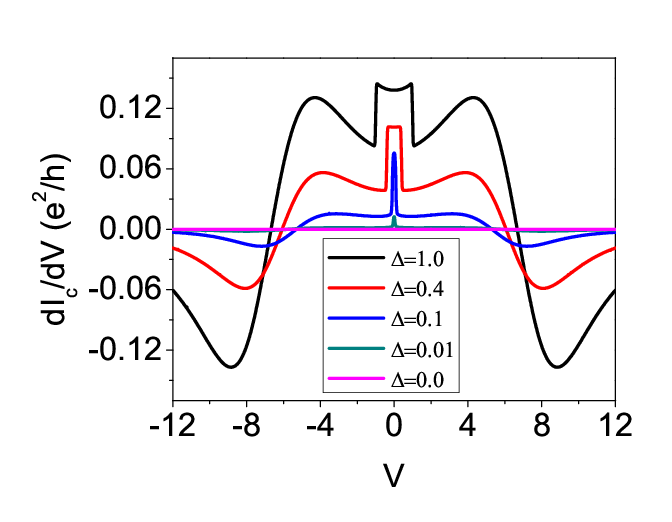
To explore the physical properties of the plateau in charge conductance, we come to study the variance of the plateau with and . Fig. 3 shows the conductance versus the spin bias for different at and . When , for any and no plateau appears. With increasing from zero, rises very quickly. The plateau begins to form when is about a few . Its width is and its height depends on weakly. This plateau remains robust even when reaches about . At a larger , a slightly downward bend emerges in the center of the plateau.

Fig. 4 shows the -dependence of the conductance versus the spin bias at . The conductance plateau always exists and is robust when , i.e. in the Kondo regime where the electron is localized in the QD. With increasing , the electron is partially delocalized leading to the plateau distorted. When the system is in the mixed-valence regime, i.e., , the plateau disappears completely, but the two sharp jumps still survive at , and a deep valley emerges at . In fact, the linear charge conductance is intensively dependent on in the mixed-valence regime. The inset of Fig. 4 plots versus , in which a deep dip exhibits at about and can even change its sign. At last, when , the QD is in an empty state, and the - curve becomes relatively smooth due to the nonexistence of the exchange process at . This behavior suggests that the conductance plateau in the Kondo regime is closely related to the localization of electron in the Kondo regime, and the physics behind the plateau deserves further discussion.

Finally we come to discuss the combined effect induced by the spin and charge bias. Consider the spin bias and the charge bias , i.e., and . In this case both spin and charge current through the QD are non-zero. Fig. 5 plots the - curve for different charge bias voltages . The results exhibit very well the combination of the plateau and the peak. The peaks are of Kondo type induced by charge bias. For a small (see Fig. 5(a)), in addition to the plateau, two extra Kondo peaks and dips begin to emerge in the - curve at the positions . The Kondo dips originate from the fact that the voltage difference decreases linearly with increasing of the charge bias , and the conventional Kondo peaks from the spin-down electron are transformed into the dips. On the other hand, for a large (see Fig. 5(b)), the Kondo peaks and dips become dominant.
4 Summary
In summary, a conductance plateau emerges in the charge differential conductance - curve in quantum spin transport, instead of the Kondo-double peak in quantum charge transport. The conductance plateau and Kondo peak are complementary to each other, and reflect the spin and charge aspects of the exchange processes in quantum electron transport.
Acknowledgements.
This work was supported by the Research Grant Council of Hong Kong under Grant No.: HKU 7041/07P (S.Q.S.); and NSF-China under Grant Nos. 10474125 and 10525418 (Q.F.S.).References
- [1] \NameKouwenhoven L. P., Glazman L. \REVIEWPhysics World14200133; J. Konig, J. Martinek, J. Barnas and G. Schon, Lecture Notes in Physics Vol. 658, P145-164 (Springer, 2005).
- [2] \NameNg T. K., Lee P. A. \REVIEWPhys. Rev. Lett.6119881768; \NameGlazman L. I., Raikh M. E. \REVIEWJETP Lett.471988378.
- [3] \NameMeir Y., Wingreen N. S., Lee P. A. \REVIEWPhys. Rev. Lett.7019932601.
- [4] \Namevan der Wiel W. G., De Franceschi S., Elzerman J. M., Fujisawa T., Tarucha S. Kouwenhoven L. P. \REVIEWRev. Mod. Phys.7520031; \NameHanson R., Kouwenhoven L. P., Petta J. R., Tarucha S. Vandersypen L. M. K. \REVIEWRev. Mod. Phys.7920071217.
- [5] \NameCronenwett S. M., Oosterkamp T. H. Kouwenhoven L. P. \REVIEWScience2811998540; \NameGoldhaber-Gordon D., Hadas Shtrikman, Mahalu D., Abusch-Magder D., Meirav U. Kastner M. A. \REVIEWNature3911998156; \NameInoshita T. \REVIEWScience2811998526.
- [6] \NameSasaki S., De Franceschi S., Elzerman J. M., van der Wiel W. G., Eto M., Tarucha S., Kouwenhoven L. P. \REVIEWNature4052000764; \Namevan der Wiel W. G., De Franceschi S., Fujisawa T., Elzerman J. M., Tarucha S. Kouwenhoven L. P. \REVIEWScience28920002105.
- [7] \NameSergueev N., Sun Q.-F, Guo H., Wang B. G., Wang J. \REVIEWPhys. Rev. B652002165303; \NameZhang P., Xue Q. K., Wang Y. P., Xie X. C. \REVIEWPhys. Rev. Lett.892002286803; \NameMartinek J., Utsumi Y., Imamura H., Barnaś J., Maekawa S., König J., Schön G. \REVIEWPhys. Rev. Lett.912003127203; \NameMartinek J., Sindel M., Borda L., Barnaś J., König J., Schön G., von Delft J. \REVIEWPhys. Rev. Lett.912003247202; \NameChoi M. S., Sanchez D., Lopez R. \REVIEWPhys. Rev. Lett.922004056601.
- [8] \NamePasupathy A. N., Bialczak R. C., Martinek J., Grose J. E., Donev L. A. K., McEuen P. L., Ralph D. C. \REVIEWScience306200486.
- [9] \NameStevens M. J., Smirl A. L., Bhat R. D. R., Najmaie Ali, Sipe J. E., van Driel H. M. \REVIEWPhys. Rev. Lett.902003136603; \NameHbner J., Rühle W. W., Klude M., hommel D., Bhat R. D. R., Sipe J. E., van Driel H. M. \REVIEWPhys. Rev. Lett.902003216601; \NameCui X. D., Shen S. Q., Li J., Ji Y., Ge W. K., Zhang F. C. \REVIEWAppl. Phys. Lett.902007242115; \NameLi J., Dai X., Shen S. Q., Zhang F. C. \REVIEWAppl. Phys. Lett.882006162105.
- [10] \NameKato Y. K., Myers R. C., Gossard A. C., Awschalom D. D. \REVIEWScience30620041910; \NameWunderlich J., Baestner B., Sinova J., Jungwirth T. \REVIEWPhys. Rev. Lett.942005047204; \NameValenzuela S. O., Tinkham M. \REVIEWNature4422006176.
- [11] \NameXing Y., Sun Q.-F., Wang J. \REVIEWPhys. Rev. B752007075324; \NameHankiewicz E. M., Li J., Jungwirth T., Niu Q., Shen S. Q., Sinova J. \REVIEWPhys Rev. B722005155305; \NameWang D.-K., Sun Q.-F., Guo H. \REVIEWPhys. Rev. B692004205312.
- [12] \NameMeir Y., Wingreen N. S. \REVIEWPhys Rev. Lett.6819922512; \NameJauho A.-P., Wingreen N. S., Meir Y. \REVIEWPhys. Rev. B5019945528.
- [13] \NameHaug H., Jauho A.-P. \BookQuantum Kinetics in Transport and Optics of Semiconductors \PublSpringer-Verlag, Berlin Heiderberg \Year1996.
- [14] \NameNg T. K. \REVIEWPhys. Rev. Lett.761996487.
- [15] \NameSun Q.-F., Guo H. \REVIEWPhys. Rev. B662002155308.
- [16] \NameKatsura H \REVIEWJ. Phys. Soc. Jpn762007054710; \NameSchiller A, Herschfield S \REVIEWPhys. Rev. B58199814978.