Spin-dependent scattering in a silicon transistor
Abstract
The scattering of conduction electrons off neutral donors depends sensitively on the relative orientation of their spin states. We present a theory of spin-dependent scattering in the two dimensional electron gas (2DEG) of field effect transistors. Our theory shows that the scattering mechanism is dominated by virtual transitions to negatively ionized donor levels. This effect translates into a source-drain current that always gets reduced when donor spins are at resonance with a strong microwave field. We propose a model for donor impurities interacting with conduction electrons in a silicon transistor, and compare our explicit numerical calculations to electrically detected magnetic resonance (EDMR) experiments. Remarkably, we show that EDMR is optimal for donors placed into a sweet spot located at a narrow depth window quite far from the 2DEG interface. This allows significant optimization of spin signal intensity for the minimal number of donors placed into the sweet spot, enabling the development of single spin readout devices. Our theory reveals an interesting dependence on conduction electron spin polarization . As increases upon spin injection, the EDMR amplitude first increases as , and then saturates when a polarization threshold is reached. These results show that it is possible to use EDMR as an in-situ probe of carrier spin polarization in silicon and other materials with weak spin-orbit coupling.
pacs
72.25.Dc; 76.30.-v. 85.75.-dI Introduction
Electron spins carry much promise as state variables for scaled classical logic[1] and as quantum bits (qubits) in quantum computer architectures.[2] A key challenge of current research in spin-based electronics (“spintronics”) and quantum computation is to devise methods to probe spin polarization in semiconductors with weak spin-orbit coupling,[3] like silicon and silicon-germanium alloys. Silicon combines many special features that make its electronic spin a promising basis for classical and quantum logic devices: Band structure properties such as weak spin-orbit coupling and indirect band gap, and the possibility of preparing a nuclear spin free environment lead to extremely long spin relaxation times in comparison to other semiconductors.[4]
However, the same features that lead to long spin relaxation times also make spin detection more challenging. Optical methods for spin detection such as Faraday and Kerr rotation have been used successfully in III-V semiconductors,[5, 6] but unfortunately, these methods are inapplicable to silicon and related materials, whose spin-selective optical transitions are extremely weak and ineffective.

Recently, injection and detection of conduction electron spin polarization was demonstrated in silicon. In Ref. [7], a Si device with a ferromagnetic (FM) source was interfaced with GaAs to enable optical spin detection, while in [8] a spin valve based on a FM-Si interface was used.
Both experiments achieve spin detection at the interface, but no local or “in-situ” spin detection. The interface limits spatial resolution and introduces additional scattering effects. In studies with accumulation channel silicon transistors, spin-dependent scattering was demonstrated by electrical detection of magnetic resonance (EDMR).[9, 10]
In this article we present a theory of spin-dependent transport in the scattering of spin polarized conduction electrons in the two dimensional electron gas of field effect transistors. Based on the scattering theory, we propose a donor-based approach to the problem of in-situ carrier spin detection in silicon. At the limit of a single donor impurity, this mechanism also provides a path for the readout of single donor spin states that does not require proximity to (or presence of) charge traps.[2, 11, 12, 14]
Consider a silicon transistor with a series of different group V donor impurities implanted along its conduction channel, Fig. 1. Spatially resolved characterization of carrier spin polarization is obtained by measuring the source-drain current when each donor species is in resonance with a microwave field.
This is possible due to spin-dependent scattering (SDS), which relies solely on the symmetry of impurity scattering events.[20, 21, 9] While this effect was believed to be observed through EDMR in [9] amidst competing heating effects, it was only recently that SDS was confirmed experimentally using a small ensemble () of implanted antimony (Sb) donors.[10] In the following, we present a general microscopic theory of SDS, its efficiency and tunability in a two dimensional electron gas (2DEG). We show that the core physical mechanisms underlying SDS are virtual transitions mediated by negatively ionized donor levels. Our results apply to all semiconductors, but are particularly useful as a probe of spin polarization in group IV and related materials with weak spin-orbit coupling, whose spin detection is intrinsically challenging. Our physical optimization of this effect has exciting consequences for spintronics and single donor electron or nuclear spin readout.[22]
We remark that SDS is quite different from other EDMR experiments based on spin-dependent recombination of electron-hole pairs.[13, 14, 15, 16, 17, 18, 19] As showed by Kaplan, Solomon, and Mott,[14] spin-dependent recombination has important contributions that do not depend on carrier spin polarization . Hence it is difficult to use recombination based EDMR as a probe of carrier spin polarization .
This article is organized as follows. Section II presents a general theory of SDS and its detection by EDMR in the case of thermal equilibrium in an external magnetic field (no spin injection). Section III describes our explicit numerical calculations, together with a comparison between theory and two experiments,[9, 10] and a discussion on how SDS can be optimized with respect to donor impurity location. Section IV discusses the validity of our perturbation theory approach, by showing explicit calculations of the Kondo temperature as a function of donor impurity location. Section V generalizes our theory to the case of non-equilibrium spin injection, and discusses how EDMR scales with carrier spin polarization. Section VI presents our conclusions.

II Theory of spin-dependent impurity scattering and electrically detected magnetic resonance
Impurity scattering depends on whether the two-particle states formed by a conduction and an impurity electron are in a singlet (S) or triplet (T) configuration,
| (1) |
Here and are orbital wavefunctions, respectively of a conduction electron with momentum in the -th subband, and a localized donor impurity electron in the ground state. Fig. 2 shows the band diagram and potential profile for conduction and impurity wavefunctions in the 2DEG.
Access to additional channels for virtual scattering in the singlet state (Fig. 3) translates into distinct neutral impurity scattering times for triplets vs. singlets, . With spin polarizations , for conduction () and impurity () electrons, the occupation fraction for singlets is given by , and the fraction for triplets . Due to this difference in singlet vs. triplet scattering times, the device current is directly related to the spin polarizations according to
| (2) |
Here we introduced the parameter as a figure of merit for the SDS effect. Eq. (2) forms the basis of the SDS mechanism of EDMR detection, which only occurs when the carrier spin polarization is non-zero. At thermal equilibrium, and in the low temperature “degenerate limit” (), arises due to Pauli paramagnetism,
| (3) |
Here , is the electron density for spin species , is the external magnetic field, (sG)-1 is the free electron spin gyromagnetic ratio, and , are the 2DEG subband ground state energies.

Under microwave irradiation, the donor spin transition rates are given by (the subscript refers to the initial state of the transition),
| (4) |
where is the amplitude of the microwave field, is the resonance frequency of the donor with nuclear spin state ( is a hyperfine shift), and is the inhomogeneous linewidth. The microwave rate competes with the donor spin-flip rate in order to determine a steady state impurity spin polarization,
| (5) |
where is the equilibrium donor spin polarization.
When donor atoms are at resonance (), and satisfy the saturation condition , their spin polarization vanishes, , effectively reducing the device current by . In the “clean limit”, when no other scattering sources are competing with donor impurity scattering, the figure of merit is given by
| (6) |
where we added a subscript to account for different subbands. Note that the saturation condition depends critically on the microwave amplitude , donor spin-flip rate and resonance linewidth .
In transport measurements, SDS is always in competition with other scattering sources, such as surface roughness and lattice defects. We describe these phenomenologically by adding a rate : . Usually, transport is dominated by scattering sources other than neutral donors (), leading to a reduced figure of merit .
The scattering amplitudes to second order in the Born approximation are given by
| (7) | |||||
and the scattering rates due to a single donor impurity are
| (8) | |||||
where is the angle between incoming () and outgoing () conduction electron wavevectors, with averaged over the Fermi distribution. In the degenerate limit we may set equal to the Fermi wavevector , but a more general averaging procedure will be considered below. Here is the 2DEG energy density, with the 2DEG area. The energy of the conduction electrons is assumed to be , with , the effective mass, and the ground state energy of the -th subband. Eqs. (7) and (8) do not depend explicitly on electron Zeeman energy because we assumed that the -factor of the donor is the same as the -factor of the electrons [while it is essential to consider different -factors for EDMR detection, e.g. in Eq. (4), the -factor differences give only a negligible effect in the calculation of transport properties, provided the external field is not too large].
The second order contribution in Eq. (7) is a sum over virtual (intermediate) states, and is generally much larger than the 1st order contribution. Fig. 3 illustrates the most important channels for neutral impurity scattering. These depend on the two-particle Hamiltonian only through the donor single-particle orbital energies , donor “on-site” Coulomb repulsion , and the overlap between conduction and impurity wavefunctions. The largest individual contribution is a virtual transition to , which is a negatively ionized donor level with two electrons in the ground orbital state [Fig. 3(a)]. This transition is only allowed for singlets due to Pauli exclusion. Since singlet scattering also has the channels for excited orbital states available, it is always stronger than triplet scattering (which has access only to the excited states) and in general .
In these neutral donor scattering events, the total spin of conduction and donor electrons is always conserved, but their respective spin states may be exchanged.[23, 24] In our notation, is the rate for a donor with spin to exchange spin with a conduction electron having spin ; using to denote the spin state, the rates can be written as
| (9) | |||||
Here are exchange scattering amplitudes, and
| (10) |
are Fermi functions. After converting the sums into integrals over space, the donor spin-flip scattering rate becomes
| (11) |
As a check, note that the equilibrium donor spin polarization is given by . When , scales linearly with the temperature, while in the opposite regime it scales linearly with .
When other donor spin-flip mechanisms are active, we must add their rate to Eq. (9). Nevertheless, we will see below that exchange scattering is the dominant contribution for donors in silicon in a wide parameter range.
III Model calculations and comparison to experiment
III.1 Model Hamiltonian and virtual two-particle donor states
The two-particle Hamiltonian that models the coupling between a conduction plus a donor impurity electron can be written explicitly as
| (12) |
where for notational simplicity denotes coordinate , and denotes coordinate . Here is the translational invariant single-particle Hamiltonian, with the kinetic energy and the 2DEG confinement (triangular at low but flattens out at high , see Fig. 2). is the attractive Coulomb potential of the impurity, and is the Coulomb electron-electron repulsion,
| (13a) | |||||
| (13b) | |||||
where is the location of the donor impurity, and the dielectric constant for silicon. Since we are in the degenerate limit, it is important to account for screening; we use Thomas-Fermi screening with wavevector
| (14) |
where is the 2DEG density and the subband wavefunction defined below. Note that the last term in Eq. (12) is the chemical potential times the number of particles.
In order to compute the scattering amplitudes [Eq. (7)], we need to choose a set of virtual states that forms a complete basis for the two-particle Hilbert space. An important insight is that the conduction electron may hop into the impurity site, form a negatively ionized virtual donor state, and then hop back into the Fermi sea. This motivates the choice of a molecular orbital basis of negatively ionized donor states:
| (15) |
where is a donor orbital state with single particle energy , satisfying . Note that refers to the ground orbital state, and refers to other excited donor single-electron orbitals. From Eq. (15) we see that the state only exists as a singlet, .
III.2 Microscopic model for single particle states and overlap integral
Bulk silicon has a six-fold degenerate conduction band, with energy minima located at along the set of directions in the Brillouin zone. Its effective mass is anisotropic. Each valley has a heavy mass equal to along the valley direction, and a much lighter mass in the perpendicular plane ( is the free electron mass). In the presence of a (001) interface, electrons in the valleys along will have considerably lower energy, a consequence of the heavy longitudinal mass.[26] This leads to the following two-subband model for the conduction electron wavefunctions: , with the 2DEG area and a subband label. The subband wavefunctions are given by and . For , we use the Takada-Uemura envelope function,
| (17) |
that is known to be an excellent analytic approximation to the self-consistent 2DEG ground state (see p. 468 of Ref. [26]). We assume for . The characteristic length scale models the 2DEG width, that can be controlled electrically by the gate voltage. Our choice of corresponds to pure imaginary intervalley scattering at the interface (other choices of intervalley scattering phase simply give a phase shift to the cosine and sine functions, that is equivalent to changing the position of the interface).[27] The conduction electron states are assumed to satisfy , where . Each subband has energy at , with valley-splitting K depending on interface quality and device geometry.[28, 29]
We now discuss model wavefunctions for the donor impurity. We expect that donors located too close to the interface will have quite high , and the EDMR saturation condition will not be satisfied. For this reason, we expect that only donors located far enough from the interface (at depths ) can contribute to EDMR. Therefore it is sufficient to use donor wave functions that are good approximations in the bulk. Those are the Kohn-Luttinger wavefunctions,[30]
| (18) |
For simplicity, we used an isotropic envelope , with . The Bohr radius depends on the hydrogenic principal quantum number according to (we used Å). The principal quantum number relates to the subscript according to . Below we will list the donor energy levels with the zero of energy chosen at flat band (the bulk conduction band edge).
The valley vectors are given by , , , , , and . The corresponding are conveniently written as 6-dimensional vectors. Each hydrogenic envelope has six different valley-split states, classified by symmetry. The lowest energy state for Sb has meV with A1 symmetry, .[31] This is followed by a three-fold degenerate T1 symmetry level, with energy meV and , , . Note that only the last state couples to the (001) subbands. The highest energy level has E symmetry with energy meV and is two-fold degenerate, , or . Again, only one of these couples to electrons in the lowest energy subband. For principal quantum number we assumed with degenerecence . Finally, we used meV for the on-site Coulomb repulsion. This corresponds to a binding energy of meV; this is quite similar to the binding energy of meV measured for phosphorous (P) in silicon,[32] and calculated by Oliveira and Falicov.[33] We are not aware of measurements of for Sb impurities.
One important point is that the overlap integral between conduction electrons in the -th valley and the impurity electron is strongly oscillatory on R. For notational convenience, define , and , and set . After a simple calculation we see that apart from a smooth envelope whenever the valley symmetry of donor orbital is “even” (), and when the valley symmetry of orbital is “odd” (). These oscillations occur due to valley interference, in a similar fashion as the exchange oscillations between two donor impurities in silicon.[34, 35, 36]
III.3 Contributions to the scattering amplitude
We start by evaluating explicitly the first order contributions to Eq. (7). To get an idea of the order of magnitude of each contribution, we will quote numerical values for a single donor located at , with parameters , meV, meV, and Å. In this case the overlap integral between conduction electron at and donor ground state was , with .
Let’s consider the first order contribution to Eq. (7). Using and , we get
| (19) | |||||
The first contribution on the right hand side is attractive Coulomb potential scattering (always negative), and the second contribution is repulsive scattering from the donor electron cloud. This has the same order of magnitude as the first term, but the opposite sign. Assuming (maximum value) these terms are respectively neV, and neV. The first term inside the brackets equals neV, the second neV, and the third neV. Hence we have neV, and neV. Interestingly, in this particular case the first order contribution to Eq. (7) favors triplet scattering. Actually, computations for different donor positions shows that the first order contribution changes sign several times as the donor position is varied.
We now turn to second order contributions to Eq. (7). We remark that these are always negative for singlets and for triplets because for . The largest individual contribution is a virtual transition to a negatively ionized donor state with two electrons occupying the donor ground state. This contributes exclusively to singlet scattering. Using Eq. (16) we get
| (20) |
which equals neV for the particular case considered. This is more than times larger than the 1st order contribution mentioned above. We checked several other parameter regimes, and found Eq. (20) to be 2-10 times larger than the 1st order contribution (singlet or triplet).
All the other second order terms contribute equally to singlet and triplet. The largest of these involve virtual excited states to the state with T1 or E symmetry. The T1 state contribution is
| (21) |
and the E contribution is
| (22) |
The contributions with principal quantum number may be lumped together in a sum:
| (23) | |||||
since there are orbitals coupling to the 2DEG valleys, each with energy . The envelope of the overlap integrals is defined as
| (24) |
We get neV, neV, neV, neV, neV, neV. The reach a maximum for , and then decrease appreciably with increasing because the ’s become exponentially small. As a result, we get a good approximation by evaluating the sum up to . We found that the contributions for produce negligible changes to our final result.
Hence the sum of the second order contributions in Eq. (7) can be as much as times larger than the first order contributions. It is interesting to note that the difference between singlet and triplet rates is determined by the difference between squared amplitudes: , which is of the order of neV2. This is several orders of magnitude larger than the square of the exchange scattering amplitude, that determines exchange scattering: is only about neV2. Therefore, we see that exchange scattering is quite different than SDS, in the sense that the latter benefits from a large number of additional electronic transitions.
III.4 Dependence of EDMR parameters on donor depth
We now show explicit numerical calculations of the parameters determining EDMR detection, and discuss their dependence with donor depth . The figure of merit is shown in Fig. 4, and the donor spin flip rate due to the exchange scattering mechanism is shown in Fig. 5. Both and decrease appreciably as increases relative to the 2DEG thickness , and are quite sensitive to (or, equivalently, the 2DEG area density). We used meV, and considered two different cases: Valley degenerate with meV, and valley-split with meV and meV. Both and are independent of the 2DEG area ; depends sensitively on the scattering time due to other sources; we used ps which is equivalent to a typical transistor mobility of cm ( is independent of ). We assumed K and T ( does not depend on , and is nearly independent of in the valley degenerate case).
Fig. 5 shows that exchange scattering is several orders of magnitude stronger than conventional spin-phonon coupling of isolated donor impurities. For example, Feher and Gere[37] measured s-1 for phosphorous donors in bulk silicon at K and T.
Interestingly, the EDMR amplitude depends on whether the device temperature is larger than the valley-splitting energy or not. At large temperatures (or small valley splittings), and are smooth functions of (apart from tiny oscillations), because contributions from the two subbands complement each other (dark curves). For the opposite regime of temperature lower than valley-splitting, the parameters are strongly oscillatory on (grey curves). In this case becomes quite small for some donor positions close to the interface, suggesting that a fraction of the donors located at “lucky sites” might be detectable by EDMR. In Figs. 4 and 5 we used filled circles to denote the actual silicon lattice sites that may be occupied by substitutional donors.


| Experiment | Theory | ||
| () | (G) | () | () |
| 1.1 | 0.3 | 10 | 5.6 |
| 2.2 | 0.3 | 4.0 | 2.2 |
| 3.8 | 0.3 | 2.0 | 0.5 |
| 2.2 | 0.07 | 1.0 | 0.5 |
| 2.2 | 0.14 | 2.5 | 1.0 |
| 2.2 | 0.19 | 3.5 | 1.4 |
| 2.2 | 0.28 | 4.0 | 2.1 |
| 2.2 | 0.55 | 5.0 | 3.8 |
III.5 Comparison to experiment
Our theory can be directly compared to experiments. Ghosh and Silsbee[9] measured at high power (the current increased upon resonance), while at lower power they found that changed sign. In this study, a silicon transistor bulk doped with phosphorous impurities was used. Lo et al.[10] measured much lower amplitudes , with antimony donors implanted only into the transistor channel. Unfortunately the use of derivative detection did not allow the determination of the sign of .
Our theory disagrees in sign with the measurements of [9], suggesting that their high power signal was not due to the SDS mechanism, instead it was likely due to the 2DEG heating mechanism.[38]
We now compare our explicit numerical results with the experimental data of Lo et al.[10] Our theory allows the prediction of the device current for a given donor distribution without any fitting parameters. Denote the number of donor impurities located in the interval , with the volume density of donors in the -thick layer. The EDMR signal averaged over the donor profile is simply given by
| (25) |
We obtained the depth dependent donor density from Secondary Ion Mass Spectroscopy measurements (SIMS). Our explicit model calculations of the EDMR current are shown in Table 1 for all measurements made in [10]. The EDMR response predicted by theory is in reasonable agreement with experiment.
III.6 Physical optimization of EDMR

Table 1 shows that the SDS contribution to EDMR is much weaker than anticipated on the basis of previous measurements.[9] We now describe a physical optimization that aims at maximizing for the minimal number of donor impurities.
The SDS parameters and decrease rapidly with increasing donor depth , an effect that has important implications for the optimization of the EDMR amplitude. Notably, for given , the EDMR signal will be maximal for donors satisfying . The location is the closest one to the interface that satisfies the saturation condition .
Fig. 6 shows the EDMR amplitude as a function of donor location, for a single donor implanted in the center of a transistor of area . We assumed microwave amplitude G, 2DEG density cm2, with other parameters as in Table I.
Interestingly, the EDMR amplitude depends on whether the device temperature is larger than the valley-splitting energy or not. At large temperatures, is a smooth function of , because contributions from the two subbands complement each other. In this case a single donor placed at the sweet spot is optimally detected by EDMR (dark curve in Fig. 6, with meV). For the opposite regime of temperature lower than valley-splitting, is strongly oscillatory on , and donors closer to the interface can be detected as well (oscillating gray curve in Fig. 6, with meV and meV).
Fig. 6 shows that EDMR is able to detect a single donor spin implanted in a transistor of area . For typical A, current modulations pA are detectable with standard techniques, provided the donor is placed at the sweet spot . A single donor resonance may be identified by the presence of only one hyperfine satellite line out of the full satellite spectrum with 2I+1 lines (for donor nuclear spin I), for measurements within the nuclear spin-flip time.[22]
The EDMR amplitude is directly proportional to the donor area density per monolayer. Therefore, if Sb donors were to be placed exactly at the sweet spot in a large transistor of area , the signal would be , two orders of magnitude higher than in [10].
IV Kondo temperature and validity of perturbation theory
Our approach is based on perturbation theory [Eq. (7)]. This is known to be a good approximation only when the temperature is larger than the characteristic Kondo temperature . For our problem, the Kondo temperature may be written as[25]
| (26) |
where is an average exchange energy at the Fermi level (averaged over subbands), and is taken as the lowest subband energy. Eq. (26) applies when and . The first term in the square root is a characteristic particle excitation bandwidth for electrons tunneling into the donor, while the second term is a hole excitation bandwidth.
Fig. 7 shows our calculated Kondo temperature as a function of donor depth. Here we see that for , we have K. Hence, even at the lowest temperatures achievable experimentally, there is no Kondo effect for donors located at ().
In the valley degenerate regime, only donors around can be detected by EDMR, as shown in Fig. 6 (donors closer to the interface can be detected at higher power). Hence we see that donors located in this region satisfy for the lowest temperatures achievable in the laboratory, and our perturbation theory approach is justified. In the valley degenerate case, both the EDMR current as well as the Kondo temperature are strongly oscillatory with donor depth, and again it can be seen that all donors that are detectable by EDMR have extremely low . Note that the behavior of as a function of donor depth is qualitatively similar to exchange scattering; as a consequence, all donors with low enough to be detectable by EDMR have a corresponding quite small .

V Spin injection
We now discuss the spin injection regime. Under spin injection, each spin species have different quasi-Fermi energies, .[1] For , the carrier polarization is well approximated by
| (27) |
Here is the 2DEG area density for each spin subband.
The impurity scattering times must now be calculated for each spin subband:
| (28) |
where we added a spin subscript to the scattering times and the Fermi functions. The energy integrals are from to . The current is now calculated as in Eq. (2), using for the spin up subband, and for the spin down subband, with in each case. In addition, each must be multiplied by its corresponding density . The source-drain current becomes
| (29) |
Interestingly, under spin injection the scattering times are intertwined with the densities , and a figure of merit independent of can not be defined. Note that when , Eq. (29) becomes , as obtained previously.
The donor spin transition rates are also modified. Following from Eq. (9), , leading to
| (30) | |||||
The steady state impurity polarization becomes
| (31) |
Fig. 8 shows EDMR lineshapes under spin injection, using K, G, and doping profile and other parameters similar to [10]. The 2DEG density is fixed at cm-2, and the conduction electron spin polarization is varied between 2% and 75%. At low , the EDMR amplitude scales as , since remains unchanged and scales proportional to due to exchange scattering [Eq. (31)]. In this regime, EDMR can be used as a local probe of carrier spin polarization.
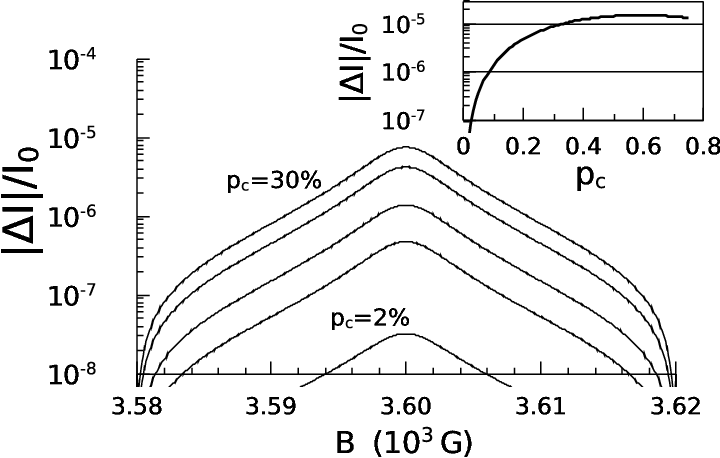
However, as is increased beyond the threshold
| (32) |
the spin-flip rate starts increasing as , because any donor spin antiparallel to the 2DEG spins will relax rapidly [note that Eq. (30) becomes proportional to when ]. By virtue of these larger ’s, EDMR will excite donors further away from the interface, tending to decrease . Remarkably, this effect competes against the scaling, saturating for . While this limits EDMR as a probe of carrier spin for , it also demonstrates that EDMR detection is optimal at .
VI Conclusions
In conclusion, we presented a microscopic theory of spin-dependent scattering in the interaction of conduction electrons with neutral donor atoms. Our results are based on an effective mass approximation. More sophisticated approaches are likely to reduce the valley oscillations,[36] with no modification to our conclusions. The considered mechanism requires temperatures lower than the impurity binding energy ( K), but even higher temperatures may be achieved using deep level magnetic atoms or clusters.
We showed that SDS is determined by virtual transitions into doubly occupied donor states. As a result, SDS always leads to a reduced current upon EDMR saturation, since .
A recent experiment[39] demonstrates that the EDMR current due to SDS is indeed reduced upon donor spin saturation (Fig. 2(c) in [39]), in agreement with our proposed virtual transition mechanism.
Spin-dependent scattering detection is challenging due to competing heating effects,[9] which are directly proportional to the number of donors present. Our finding that SDS arises solely from impurity spins located within a narrow depth window with respect to the 2DEG shows a path to significant optimization of spin signal intensity for a minimal number of donors placed into this depth window, and underpins the development of single spin readout devices.
Our theory shows how the EDMR amplitude will scale with carrier spin polarization in the regime of spin injection.[3, 7, 8] Therefore, the monitoring of donor electron spin resonances can be utilized for the spatially resolved characterization of conduction electron spin polarization, providing a sensitive probe for optimization of spin injection and spin transport in semiconductors with indirect band gap and weak spin-orbit coupling.
We thank M. Friesen, T. Schenkel, A.M. Tyryshkin, and I. Žutić for a careful reading of the manuscript, and A.L. Efros, X. Hu, B. Koiller, S.A. Lyon, I. Martin, J.E. Moore, and A.G. Petukhov for useful discussions. RdS acknowledges support from NSERC and the UVic Faculty of Sciences; CCL and JB acknowledge support from WIN and NSA.
References
- [1] I. Žutić, J. Fabian, and S. Das Sarma, Rev. Mod. Phys. 76, 323 (2004).
- [2] B.E. Kane, Nature 393, 133 (1998).
- [3] I. Žutić, J. Fabian, and S.C. Erwin, Phys. Rev. Lett. 97, 026602 (2006).
- [4] A.M. Tyryshkin, S.A. Lyon, A.V. Astashkin, and A.M. Raitsimring, Phys. Rev. B68, 193207 (2003).
- [5] J.M. Kikkawa and D.D. Awschalom, Nature 397, 139 (1999).
- [6] S.A. Crooker, M. Furis, X. Lou, C. Adelmann, D.L. Smith, C.J. Palmstrøm, and P.A. Crowell, Science 309, 2191 (2005).
- [7] B.T. Jonker, G. Kioseoglou, A.T. Hanbicki, C.H. Li and P.E. Thompson, Nature Physics 3, 542 (2007).
- [8] I. Appelbaum, B. Huang, and D.J. Monsma, Nature 447, 295 (2007).
- [9] R. N. Ghosh and R.H. Silsbee, Phys. Rev. B46, 12508 (1992).
- [10] C.C. Lo, J. Bokor, T. Schenkel, J. He, A.M. Tyryshkin, and S.A. Lyon, Appl. Phys. Lett. 91, 242106 (2007).
- [11] M. Xiao, I. Martin, E. Yablonovitch, and H.W. Jiang, Nature 430, 435 (2004).
- [12] J.M. Elzerman, R. Hanson, L.H. Willems van Beveren, B. Witkamp, L.M.K. Vandersypen, L.P. Kouwenhoven, Nature 430, 431 (2004).
- [13] D.J. Lepine, Phys. Rev. B6, 436 (1972).
- [14] D. Kaplan, I. Solomon, and N.F. Mott, J. Phys. (Paris), Lett. 39, L51 (1978).
- [15] P. Christmann, W. Stadler, and B.K. Meyer, Appl. Phys. Lett. 66, 1521 (1995).
- [16] M.S. Brandt, S.T.B. Goennenwein, T. Graf, H. Huebl, S. Lauterbach, and M. Stutzmann, phys. stat. sol. (c) 1, 2056 (2004).
- [17] A.R. Stegner, C. Boehme, H. Huebl, M. Stutzmann, K. Lips, and M.S. Brandt, Nature Physics 2, 835 (2006).
- [18] D.R. McCamey, H. Huebl, M.S. Brandt, W.D. Hutchison, J.C. McCallum, R.G. Clark, and A.R. Hamilton, Appl. Phys. Lett. 89, 182115 (2006).
- [19] G.W. Morley, D.R. McCamey, H.A. Seipel, L.-C. Brunel, J. van Tol, and C. Boehme, Phys. Rev. Lett. 101, 207602 (2008).
- [20] A. Honig, Phys. Rev. Lett. 17, 186 (1966).
- [21] J. Schmidt and I. Solomon, C.R. Acad. Sci. B 263, 169 (1966).
- [22] M. Sarovar, K.C. Young, T. Schenkel, and K.B. Whaley, Phys. Rev. B78, 245302 (2008).
- [23] G. Bastard and L.L. Chang, Phys. Rev. B41, 7899 (1990).
- [24] G.D. Mahan and R. Woodworth, Phys. Rev. B78, 075205 (2008).
- [25] F.D.M. Haldane, J. Phys. C 11, 505 (1978).
- [26] T. Ando, A.B. Fowler and A. Stern, Rev. Mod. Phys. 54, 437 (1982).
- [27] L.J. Sham and M. Nakayama, Phys. Rev. B20, 734 (1979).
- [28] K. Takashina, Y. Ono, A. Fujiwara, Y. Takahashi, and Y. Hirayama, Phys. Rev. Lett. 96, 236801 (2006).
- [29] S. Goswami, K.A. Slinker, M. Friesen, L.M. McGuire, J.L. Truitt, C. Tahan, L.J. Klein, J.O. Chu, P.M. Mooney, D.W. van der Weide, R. Joynt, S.N. Coppersmith and M.A. Eriksson, Nature Physics 3, 41 (2007).
- [30] W. Kohn, Solid State Physics, Vol. 5, 257 (1957).
- [31] H.G. Grimmeiss, E. Janzén, and K. Larsson, Phys. Rev. B25, 2627 (1982).
- [32] S. Narita, Solid State Commun. 53, 1115 (1985).
- [33] L.E. Oliveira and L.M. Falicov, Phys. Rev. B33, 6990 (1986).
- [34] P.R. Cullis and J.R. Marko, Phys. Rev. B1, 632 (1970).
- [35] B. Koiller, X. Hu and S. Das Sarma, Phys. Rev. Lett. 88, 027903 (2001).
- [36] C.J. Wellard and L.C.L. Hollenberg, Phys. Rev. B72, 085202 (2005).
- [37] G. Feher and E.A. Gere, Phys. Rev. 114, 1245 (1959).
- [38] D. Stein, K.v. Klitzing, and G. Weimann, Phys. Rev. Lett. 51, 130 (1983).
- [39] L.H. Willems van Beveren, H. Huebl, D.R. McCamey, T. Duty, A.J. Ferguson, R.G. Clark, and M.S. Brandt, Appl. Phys. Lett. 93, 072102 (2008).