Sub-10ps Monolithic and Low-power Photodetector Readout
Abstract
Recent advances in photon detectors have resulted in high-density imaging arrays that offer many performance and cost advantages. In particular, the excellent transit time spread of certain devices show promise to provide tangible benefits in applications such as Positron Emission Tomography (PET). Meanwhile, high-density, high-performance readout techniques have not kept on pace for exploiting these developments.
Photodetector readout for next generation high event rate particle identification and time-resolved PET requires a highly-integrated, low-power, and cost-effective readout technique. We propose fast waveform sampling as a method that meets these criteria and demonstrate that sub-10ps resolution can be obtained for an existing device.
Keywords:
Fast, picosecond timing, Time-Of-Flight readout, time-resolved PETPACS
29.40.Ka, 29.40.Mc, 87.57.ukand
1 Background
Recent developments in high-density, high precision timing photodetectors are finding applications in Cherenkov detection techniques for particle identification, as well as medical imaging applications. This is true for both traditional vacuum-based [1] (Micro-Channel Plate, Hybrid Photo-Diode) and solid state [2] (Geiger-mode APD) photodetectors, and have resulted in lower cost, higher quantum efficiency, and improved transit-time-spread (TTS) photon detection options. Fig. 1 illustrates that without these improvements, the performance of large-scale Time-Of-Flight (TOF) systems for precision spectrometers has stagnated at a resolution of about 100ps.

At the same time, the ability for electronics to resolve at the 25ps or better level has been available for decades, as reviewed in [15] and summarized in Table 1.
| Technique | Resolution [ps] | Citation |
|---|---|---|
| TDC counter | 200 (20) | [16] ([17]) |
| Vernier (Chronotron) | [18] | |
| Overlap Coin.(TAC) | [19] | |
| Start-Stop (TAC) | [20] | |
| Microwave | [21] |
For instance, consider a very simple Time to Amplitude Converter (TAC) circuit, as illustrated schematically in Fig. 2. When combined with a modest resolution ADC measurement, this is just about the simplest possible Time-to-Digital Converter (TDC). In its most reduced form the circuit consists simply of a current source, a switch, and a capacitor, as indicated in the figure.

At the start of some event of interest, the switch is closed and current starts to flow into the capacitor, which is initially at 0V. Because
| (1) |
and for constant current I, which is , one obtains
| (2) |
After the time interval , the switch opens and the voltage stored on the capacitor is a linear function of the ratio of the current over the capacitor . Note that a maximum period can be measured for a maximum voltage . Rewriting this expression we determine the time interval simply by measuring and having previously determined the current and capacitance values (or determining their ratio from calibration).
| (3) |
Putting in numbers corresponding to typical values for TOF applications and standard electronics, as listed in Table 2, one sees that
| (4) |
| Item | Value |
|---|---|
| 4.095 V | |
| Capacitor | 10 pF |
| Ramp Current | 409.5 A |
| Full scale | 100 ns (typ.) |
| ADC Resolution | 12-bits (4096 counts) |
| Noise level | 1mV |
This is conveniently at about the amplitude often observed for board-level and other system pick-up noise in large systems. Therefore, the least count of this TAC is approximately
| (5) |
and for an ideal binary interpolation of this least count, one could do even a factor of better. Non-linearites due to imperfections and temperature dependence in the current source and switch can degrade performance, but have been addressed in a number of commercial modules. For high rate environments, variants of this same basic scheme involving multiple ramps, have been employed for fast TOF measurement in an online trigger [22], as well as hit logging prior to trigger formation [23].
This performance is so much better than that for the ps limit mentioned earlier that even if the TDC contribution were made zero, the overall timing would only improve by 3ps:
| (6) |
Therefore, the culprit must reside in the method of conveying the leading edge timing of the photodetector pulse into a signal that these proven methods can use.
2 Amplitude Dependent Effects
This well-known issue of “time walk” is illustrated in Fig. 3, where a photodetector output signal shape is amplitude dependent. Time walk corrects are used to compensate for the time of a threshold crossing slews to later times for smaller pulses.

For detector signals with large amplitude variations, the effect can be quite sizeable and must be corrected. A simple and proven method is to integrate the charge of the pulse within a gate around the signal of interest. While the leading edge of the signal can be complex, and can be modelled by a power-law, the observable of interest is the dependence on the pulse-integrated charge. This is illustrated in Fig. 4, where the dependence observed for the Belle TOF system [11] is consistent with many previous observations as being proportional to approximately .

Plotted as a function of in the upper left graph of Fig. 4, this dependence appears then as a linear expression. The effect of applying the correction is shown in the lower plots, where the amplude dependence has been removed and more than a factor of 4 in timing resolution improvement is observed. However, to further reduce scatter in the distribution requires a different or better parameterization.
For signals with smaller amplitude variations, such as in single photon detection, Constant Fraction Discrimination (CFD) techniques can be used instead, and may be combined with multi-hit devices [17, 24] to achieve good timing performance. However, pile-up and rate effects need to be studied for each application. Moreover, all of the difficult work in making this circuitry functional is pushed onto the discriminator circuit. To reduce the effect of overdrive, the dependence of comparator output time upon amplitude above threshold, often a large amount of power may be required, making the circuitry difficult to densely integrate. Due to the intrinsic memory of the CFD technique, it is susceptible to pile-up effects.
A number of techniques, such as multi-level thresholding, have been proposed to directly measure the risetime and provide a compensating correction. Each threshold measurement may require an additional amplitude dependent correction to obtain the best possible timing. Adding more and more thresholding levels, one asymptotically approaches the penultimate technique, which is waveform sampling.
3 Waveform Sampling
A measurement complication at high event rates is pile-up, where the timing signal of interest may be superimposed on the tail of a preceding pulse. Without correction, and often being unaware that this superposition is present in the data, an incorrect timing determination will be made. If affordable and fast enough [25], and if the aperture jitter is small enough, waveform sampling provides maximum information extraction. The benefits may be summarized as follows:
- •
Pile-up impact extraction
- •
Fit to actual pulse shape
- •
Average to reduce single measurement errors
- •
Observe changes to pulse shape over time
where the last issue can be particularly important for detectors that undergo radiation damage or aging effects such that the intrinsic pulse shape evolves with time.
4 The BLAB1 Monolithic Sampler
To demonstrate the viability of the waveform sampling technique, we use the first Buffered LABRADOR (BLAB1) ASIC [25]. This is a (64k) cell deep waveform sampling ASIC that was developed as a deep-sampling extension of the successful LABRADOR ASIC [26]. The key parameters of this device are summarized in Table 3.
| Item | Value |
|---|---|
| Sampling Input Channels | 1 |
| Storage rows | 128 |
| Storage cells/row | 512 |
| Total storage cells | 65,536 |
| Sampling speed (GSa/s) | 0.1 - 6.0 |
| Storage record | 10.9 - 655 s |
| Operation mode | continuous storage/readout |
The evaluation system consists of the small circuitboard, containing 2 BLAB1 ASICs, and read out over USB2.0 by a laptop running a custom data acquisition program based on the wxWidgets tool kit. A photo of this compact measurement system is displayed in Fig. 5. This compact configuration can turn any PC (or laptop) into a high-performance digital signal oscilloscope.

5 Precision Timing Performance
All of the standard precision timing measurement techniques discussed at the outset suffer from practical limitations in actual application, which has served to degrade the realized large system performance. In the end, one simply cannot do better than having a high-fidelity “oscilloscope on a chip” for every sensor channel. Cost and data volume precluded this type of waveform recording until recent generations of SCA ASICs [26, 27, 28, 29, 30] demonstrated such techniques were practical, especially for large systems.
5.1 Calibration
In order to achieve fine timing resolution, a number of calibrations need to be performed and corrections need to be applied. As reported in earlier devices, the temperature dependence [25, 26] of the sampling baseline must be compensated. The effect of this temperature dependence is seen in Fig. 6.

In order to address bin-by-bin timing width differences, a couple of different calibration techniques have been tried. The first utilizes a sine wave zero-crossing technique used for calibrating the LAB3 ASIC[26]. That technique works best when the frequency of the sine wave is such that the measured interval between zero crossings can be uniquely assigned to a limited number of bins between successive crossings.

Due to sine wave curvature, this technique has an irreducible systematic error that is a function of sample rate. A more successful technique is to histogram the zero crossings of a sine wave and use the bin occupancy to derive the effective aperture width, as may be seen in Fig. 7.
When a sampling strobe is inserted into the BLAB1, the strobe propagates across a Switched Capacitor Array (SCA) row and exits the ASIC via a monitor pin. The sampling speed is determined by measured this propagation delay, a method implemented by creating a feedback loop with the insertion-extraction chain and an inverter located inside the companion FPGA. This feedback inverter is only connected after waveform readout of a triggered event and then disconnected once the sampling speed has been measured for that particular triggered event. A so-called Ripple Carry Out (RCO) period may then be expressed as
| (7) |
where the factor of 2 comes from the FGPA feedback inverter toggling the RCO period, is the SCA propagation time, and is the additional time accrued due to internal FPGA routing, circuit board routing, and routing to and from the SCA within the ASIC. To measure an FPGA-based Time-to-Digital Converter (TDC) is used [31]. Both phases of a 250 MHz clock are used by the TDC to obtain a least count of 2ns. Improved resolution is obtained by integrating the RCO period for 2048 cycles, corresponding to an aggragate single-cycle least count of 0.977 ps. is obtained by subtracting from , where is determined from a fit to a fixed frequency sinusoidal signal. The sampling speed is then
| (8) |
where is the sampling speed and is the number of SCA cells in a row, which for the BLAB1 ASIC is 512 cells. As reported in Ref. [25], the sampling timebase is temperature dependent. This effect may be seen as the correlated portion of Fig. 6. By measuring the BLAB1 timebase, these timebase shifts can be monitored and corrected offline.
5.2 Ideal Test Signals
An idealized test pulse of fixed amplitude and width was generated by taking an Agilent 33250A arbitrary waveform generator pulse output, AC coupling the signal with an inline capacitor, RF splitting the signal, and waveform sampling both signals using two separate BLAB1 ASICs with additional cable delay for the second channel. This AC coupling served as a filter and shaped the pulse into an almost gaussian shape, as seen in Fig. 8.

The result obtained for taking the time difference of a simple gaussian fit to the signals in both channels is plotted in Fig. 9.

5.3 Varying Sampling Window Position
The two pulses were then recorded without regard to the sampling strobe phase. This allows the two pulses to move around within the waveform sampling window. During the analysis, a bin-by-bin timebase correction and an event-by-event sampling speed correction were applied. The time was measured by taking the cross correlation of the two waveforms. The cross correlation was done by taking the Fast Fourier Transform (FFT) of both waveforms, complex multiplying one FFT by the complex conjugate of the other FTT, and Inverse Fast Fourier Transforming (IFFT) this product to get the cross correlation waveform in the time domain. The time position of the maximum point in the cross correlation waveform is the time difference between the best estimator of the location of the two pulses. Because the sampling speed between the two ASIC chips vary from each other and the time spacing between the bins is not constant, before FFT a fifth order data spline is applied at a fixed time spacing very close to the average time interval. This is done to keep the sampling spacing between points constant and minimize frequency domain distortion. To get finer time spacing in the cross correlation waveform without distortion, we symmetrically insert zeros in the cross correlation FFT for frequencies greater than the Nyquist frequency and less than the negative Nyquist frequency before the IFFT operation. The time resolution obtained using this technique is shown in Fig. 10, corresponding to an RMS of 6.7 RMS or a of 6.0 ps.

For complex curvature along the leading edge of the signal, the timing resolution obtained is seen to be rather sensitive to the method choosen to characterize the signal “hit” time. Unless the photodetector signal is for a single p.e. quanta, the actual shape can be rather complex and dependent upon photon arrival statistics. Even in this simple case, noise and aperture systematics upon the leading edge can be important and can also be reduced by using multiple samples to fit to an analytic signal shape. In general, the estimate error can improve as something like 1/ for N samples along the leading edge. This is perhaps the most powerful aspect of having the full waveform samples to fit. Individual sampling errors can be averaged out. Examples are provided in the following subsection, where it is clear that at the sampling rates being studied, this waveform recording technique logs many samples on the leading edge, which can be used to improve the signal timing extraction.
5.4 PMT signal observation
A convenient feature of the BLAB1 ASIC is that a PMT output transmitted over a 50 coaxial cable can be directly connected to the BLAB1 input. A waveform recorded from a Burle 85011 Micro-Channel Plate PMT is displayed in Fig. 11.
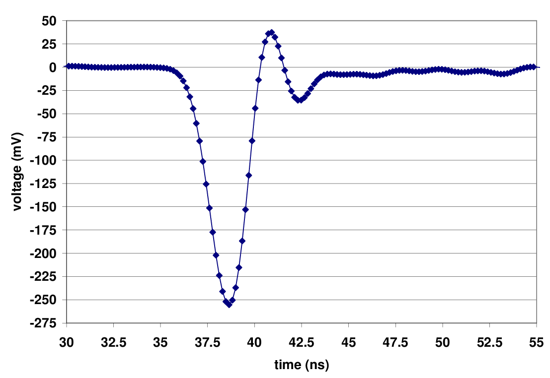
This near ideal waveform is utilized as the simulation template in the following section on performance limits from simulation.
5.5 MCP-PMT signal timing
A set of 10k triggered (cosmic and dark count) events were recorded, as illustrated for an example signal in Fig. 11. The signal amplitude was allowed to fluctuate and the measured distribution of integrated charge is shown in Fig. 12.

Ideally one would use a fast timing (ps) laser to do this measurement, however the Transit Time Spread of the photodetector would then be an issue. Instead we use the same pulse, split it, and record the signal on two storage channels. After applying timebase and time bin corrections, the raw timing difference distribution seen in Fig. 13 is obtained.

This distribution is rather wide and is related to a residual timing miscalibration. This can be seen by looking at the time difference as a function of the peak time determined on the first channel, as shown in Fig. 14.

We created a secondary bin-by-bin timing correction related to the time position of the first peak using the data from Fig. 14. After applying this secondary tinming correction, Fig. 15 illustrates the improvement in timing performance.

For this measurement, the amplitude of the MCP signal varies from event to event. For the waveform data, we calculate the charge of the signal by summing all the waveform data points, multiplying by the average timebase, and dividing by the termination resisitor. After applying all the corrections previously mentioned, a profile histogram of the charge versus time in Fig. 15 is shown in Fig. 16, which illustrates that only a slight amount of residual time walk is remains after applying the correction.

6 Limitations
While the analog bandwidth of the BLAB1 is adequate for many RF recording applications, a higher bandwidth device will be explored, based upon the lessons learned from this first device. In particular, the fanout structure and design of the analog amplifier tree is being scrutinized and improved in simulation. It is hoped that an almost arbitrarily large storage depth can be accommodated up to 1GHz of analog bandwidth through a careful layout of the buffer amplifier cascade array.
To gain insight into the parameters that are most important to attaining the highest possible timing precision, a series of simulation studies were performed. In each run a series of 10k events were generated with a time offset equal to that used in the previous section. A real pulse template shown in Fig. 11 has been used, and is perturbed as described for each of the following cases. The simulation outputs the distorted waveforms into the same data structure as used by the acquisition software and the same cross-correlation method described earlier is applied.
6.1 Random Noise
The result due to the random addition of noise to each sample of the two waveforms is illustrated in Fig. 17. Comparing the curve with the measured result, an effective noise of is indicated.

However, since we know that the noise in each sample is only about 1mV, additional contributions need to be considered.
6.2 Sample Aperture Jitter
Another expected contribution to the extraction of the timing resolution is jitter on the timing samples. Using the same simulation configuration, the sample noise is now fixed and the effect of adding a randomized aperture jitter is plotted in Fig. 18.

The local signal slope is used to determine a voltage offset expected by sampling at the wrong time. Since the sampling period is small compared with the typical voltage step between samples, a rather large jitter is needed to reproduce the observed time resolution. From direct measurements of timebase jitter, we expect a far smaller value than is required to explain the time resolution observed. It is noted that the two effects are degenerate in the sense that they lead to a sample voltage dispersion from the ideal value. Considering this, one can express the time difference resolution in terms of a combined value characterized in terms of a Signal to Noise Ratio (SNR). This relationship is seen in Fig. 19, where it is clearly seen that an effective SNR of 100 or greater is desired to obtain time resolutions of 5ps or better.

6.3 Sampling Timebase Jitter
While the pedagogical illustrations above are helpful in understanding what limits the time resolution that can be obtained, there is an additional contribution that is an artifact of the use of the BLAB1 ASIC. Specifically, it contains no dedicated Delay Lock Loop (DLL) circuitry, and thus the sampling timebase is sensitive at the level of about 0.2%/ [25]. Even though an event-by-event correction is performed, as described previously, it is quite probable that a residual correction error contributes to the time resolution. A simulation is performed as shown in Fig. 20, where 1mV of noise is added in quadrature with 1ps of sample aperture jitter on top of an overall event-by-event sampling timebase jitter. This jitter is assumed to be uncorrelated between the two ASICs.

In the limit that the known 1mV noise only contributes 2ps to the overall time resolution and that the sample aperture jitter is negligible, this effect is seen to be dominant. Quantitatively, this corresponds to about a 10% error on correcting the event-by-event sampling timebase. If true, this can be improved through better timebase stabilization in a next version of the ASIC [25], or through the use of other devices as described next.
7 Other Implementations
The waveform sampling technique described is more general than the particular ASIC presented. Indeed if price and power are no object, a number of commercial digitizers are available, with new devices continually coming to market. In general those devices, besides being rather power hungry, also suffer from a limited dynamic range. However, for many applications, they are already or will become viable.
In the near term, a number of custom ASICs with better analog resolution [32], faster sampling [33] and faster readout [34], will be available to implement these waveform sampling techniques. Further studies of the performance limits on timing signal extraction using this waveform sampling technique is a high priority for the follow-on BLAB2 ASIC [25] as well. In the longer term, these low-cost devices show great promise to replace standard ADC and TDC techniques in many future high energy and particle astrophysics detectors [35]. As we have demonstrated, they should be able to do so with excellent timing precision.
8 Summary
A waveform sampling technique has been shown to obtain sub-10ps timing resolution for readout of photodetector signals. Measurements were made with an existing compact, low-power and pipelined readout ASIC. Such a technique can be scaled up to very large channel counts in a cost-effective way.
9 Acknowledgements
The authors gratefully acknowledge the generous support of the MOSIS Educational Program, which provided the fabrication of the BLAB1 ASIC prototype through their University Research Program. Testing was supported in part by Department of Energy Advanced Detector Research Award # DE-FG02-06ER41424. This manuscript is dedicated to Sim Edward Varner, who passed away during its preparation.
References
- [1] For instance the Burle 85011 and Hamamatsu H-8500 MCP-PMTs.
- [2] For instance the Hamamatsu line of MPPCs and SenSL line of G-APDs.
- [3] T. Fazzini et al., “Electron Decay of the Pion,” Phys. Rev. Lett. 1, 247 (1958).
- [4] J. Enstrom et al., “Measurement of the Two-Photon Decay of the Meson,” Phys. Rev. D4, 2629 (1971).
- [5] T. Bressani et al., Nucl. Instr. Meth. A221 (1984) 355.
- [6] J.S. Brown et al., Nucl. Instr. Meth. A221 (1984) 503.
- [7] J.Z. Bai et al. (BES Collaboration), Nucl. Instr. Meth. A458 (2001) 627.
- [8] ibid.
- [9] Y. Kubota et al., (CLEO Collaboration), Nucl. Instr. Meth. A320 (1992) 66.
- [10] V. Sum et al., Nucl. Instr. Meth. A326 (1993) 489.
- [11] H. Kichimi, Y. Yoshimura, T. Browder, B. Casey, M. Jones, S.L. Olsen, M. Peters, J. Rodriguez, G. Varner, Y. Zheng, Y. Choi, D. Kim, J. Nam, Nucl. Instr. Meth. A453 (2000) 315.
- [12] W. Klempt, Nucl. Instr. Meth. A433 (1999) 542.
- [13] D. Acosta et al., Nucl. Instr. Meth. A518 (2004) 605.
- [14] M. Shao et al., Nucl. Instr. Meth. A558 (2006) 419.
- [15] D. Porat, “Review of Sub-nanosecond time-interval measurements”, IEEE Trans. on Nucl. Sci. Vol. NS-20, No. 5, p. 36-51 (1973).
- [16] H. Meyer, Nucl. Instr. Meth. 40 (1966) 149.
- [17] J. Christiansen et al., “A data driven high performance time to digital converter,” Proceedings of Electronics for LHC experiments, Krakow (2000) 169-173.
- [18] W.H. Venable, Jr., Rev. Sci. Instr. 37 (1966) 1443.
- [19] H. Weisberg, Nucl. Instr. Meth. 32 (1965) 138.
- [20] H. Brafman, Nucl. Instr. Meth. 34 (1965) 239.
- [21] Z.G.T. Guiragossian et al., 1973 Particle Accelerator Conf., San Francisco, CA, 1973; Report No. HEPL 705, Stanford University (1973).
- [22] D.H. Orlov et al., Nucl. Instr. Meth. A333 (1993) 513.
- [23] G. Varner et al., “A Time Expanding Multihit TDC for the Belle TOF Detector at the KEK B-Factory,” Conference Proceedings of the Sixth International Conference on Electronics for Particle Physics, P17, May 1997, pp. 28-29.
- [24] G. Varner and L. Ruckman, Journal Instr. 2 (2007) P04006.
- [25] L. Ruckman, G. Varner and A. Wong, “The first version Buffered Large Analog Bandwidth (BLAB1) ASIC for high luminosity collider and extensive radio neutrino detectors,” arXiv/0802.2278, submitted to NIM A.
- [26] G.S. Varner, L.L. Ruckman, J.W. Nam, R.J. Nichol, J. Cao, P.W. Gorham, M. Wilcox, ”The large analog bandwidth recorder and digitizer with ordered readout (LABRADOR) ASIC,” Nucl. Inst. Meth. A 583 447 (2007).
- [27] S. Kleinfelder, IEEE Trans. Nucl. Sci. 50 (2003) 955.
- [28] C. Brönnimann, R. Horisberger and R. Schnyder, Nucl. Instr. Meth. A420 (1999) 264.
- [29] S. Ritt, Nucl. Instr. Meth. A518 (2004) 470.
- [30] E. Delagnes et al., Nucl. Instr. Meth. A567 (2006) 21.
- [31] G. Varner, Journal Instr. 1 (2006) P07001.
- [32] SAM2 ASIC based on [30], E. Delagnes (DAPNIA), private communication.
- [33] 40GSa/s ASIC, J-F. Genat (Univ. Chicago), private communication.
- [34] DRS4 ASIC based on [29], S. Ritt (PSI), private communication.
- [35] G. Varner, L. Ruckman, J. Schwiening and J. Va’vra, “Compact, Low-power and Precision Timing Photodetector Readout,” PoS (PD07) 026.