Topological Aspects of Surface States in Semiconductors
Abstract
Topological aspects of surface states in semiconductors are studied by an adiabatic deformation which connects a realistic system and a decoupled covalent-bond model. Two topological invariants are focused. One is a quantized Berry phase, and the other is a number of the edge states. A winding number as another topological invariant is also considered. The surface states of Si and Ge at (111), (110), and (100) surfaces are classified by the topological invariants. Surface states of the GaAs as heterosemiconductors are also discussed.
Keywords:
semiconductor surface, Berry phase, edge state, dangling bond, Ge, Si, GaAsIntroduction
For a few decades the topological feature which does not depend on the detail of systems has been attracting attention in the condensed matter physics. One of most remarkable examples is a quantum Hall effect (QHE)[1], where a topological invariant known as the Chern number [2] has been observed experimentally. The Chern numbers are defined for a bulk state without boundaries. In the QHE, the edge states which are characteristic for a system with boundary also have a significant topological importance [3].
Edge states or surface states, which localize at a boundary of a system, have significant effects in physical phenomena; e.g., the zero bias conductance peak structure in anisotropic superconductivity [4, 5], single-layer graphite [6], and the boundary local moment at an edge of hexagonally bonded honeycomb sheets consisting of B, N, and C atoms [7]. Especially, in a graphene, it is now widely understood that there exist important edge states which are related to the chiral symmetry of the system and the Dirac cone spectrum. In metal-semiconductor interfaces, an interface state, known as the metal induced gap state, has an important role in understanding Fermi-level pinning [8].
Moreover, in realistic materials, there exists a surface reconstruction or a surface relaxation, which is sensitive to the detail of systems. However, we shall discuss that topological invariants which is independent of the detail of models is useful for understanding the surface states of 3 dimensional semiconductors. A candidate of topological invariants for semiconductors is the quantized Berry phase which has been proposed as a local order parameter for clarification of the phase of the gapped quantum liquids. It has been demonstrated that quantization of this local order parameter has an advantage over the usual order parameter in a frustrated spin system[9], and a strongly correlated system[10].
In this paper, the quantized Berry phase is evaluated for surface states in typical semiconductors such as Si, Ge, and GaAs. We note that the Berry (or Zak) phase also appears in the King-Smith-Vanderbilt formula in the theory of macroscopic polarization.[11, 12] In our case the Berry phase is defined for a 1-dimensional system with 2-dimensional wave vectors to characterize the surface, and quantized due to a anti-unitary symmetry. In addition, we focused on the number of the edge states and a winding number as the other topological invariants, following Ref.\citenRyu_Hatsugai_2002. For simplification, we limit ourselves to surface states in ideal surfaces understood as Shockley states[14]. Shockley states at a metal-semiconductor contact are closely-linked to dangling bonds.[15] Although we does not consider a surface reconstruction, the study on surface states at ideal surfaces sheds a light on real materials in the sense that the number of dangling bonds in a respective surface acts as a trigger for surface-dependent physics; for example, structures on (111) surface of Si[16] and Ge[17], structures on (110) surface of Si[18] and Ge[19], and structures on (100) surface of Si[20] and Ge[21].
Model and Results
To consider (111), (110), and (100) surfaces of Si, Ge, and GaAs as typical IV and III-V semiconductors, we use tight binding models determined by the Slater and Koster’s energy integrals[22]. We also consider a spin-orbit coupling that is important for Ge. We use the tight binding and spin-orbit coupling parameters of Grosso and Piermarocchi[23] for Ge, those of Klimeck et. al. [24] for Si, and those of Boykin et. al.[25] for GaAs. Note that a model is considered for Ge, and a model for Si, and GaAs.
To define a surface-dependent Berry phase, let us start from the definition of a bulk Hamiltonian. A position of a center of a unit cell is given by , where , , and are primitive vectors. Primitive reciprocal lattice vectors are defined by , where is the Kronecker delta. A wavenumber vector is given by . The bulk Hamiltonian in three dimensional periodic boundary condition (PBC) is given by
| (1) |
Here, the label distinguishes spin-dependent orbitals in a unit cell. We suppose two atoms in a unit cell and denote orbitals as , where is a number of orbitals in a atom and on a atom means an orbital opposite to an orbital on the other atom (See Fig. 1). Then, is a matrix.

Next, we suppose that and span a plane parallel to a surface of a semiconductor as a shaded plane shown in Fig. 1. 2-dimensional wavenumber vector is given by . Then, the bulk Hamiltonian is written as
| (2) |
where the label is defined as and is a matrix, and . is a number of layers. To consider the surface, we introduce the open boundary condition (OBC) for the one dimensional system in the direction. The matrix is given by truncating . For example, a natural way to truncation is to prohibit all the matrix elements across . We define a boundary-hopping matrix as
| (3) |
is matrix. This matrix represents all hopping elements across the boundary of the system.
To define the Berry phase, we introduce a twist angle in a hopping term across the boundary as . In detail, the twist angle is introduced in a selected element of and we denote it as . Then, the Berry phase can be defined as
| (4) |
where is the half-filled ground state of . Especially, we denote main elements of the Berry phase as . The Berry phase is quantized because the one-dimensional system at defined by has a inversion symmetry at the boundary: . When we denote the inversion as and the complex conjugate as , the anti-unitary operator is commutable with the Hamiltonian. Then, the Berry phase turns out to be quantized in the same way as in Ref.[9].
Figure 2 (a) shows the band structure of of Ge and reproduce the indirect gap.[26] After introducing the (111) surface, the band diagram of has edge states in the band gap, which are doubly-degenerated per spin, as shown in Fig. 2 (b). The Berry phase of Ge (111) surface is actually quantized and does not depend on . It turns out to be on the strongest hopping in and zero on the others. We note that the number of candidates of is 48 for the parameters we used.
(a)

(b)

The quantized Berry phase and the number of edge states are topological invariant in the following adiabatic transformation. We first modify the spin-orbit coupling term adiabatically to zero preserving the energy gap open, that is, without changing the topological invariants. At this stage the Hamiltonian is spin decoupled as . Now we ignore the spin index below for simplification. Next, we can modify the hopping terms between different orbitals and obtain a Hamiltonian as the sum of two band Hamiltonians where involves hopping terms between and only. For this process, it is also possible to hold the gap open. After the Fourier transformation of the direction, can be written as a 2 2 matrix . We can expand by the Pauli matrices by
| (5) |
where is the 2 2 identity matrix. This equation indicates a one to one mapping between and a four dimensional vector . Therefore, for fixed , a loop in space is given as varies over . We note that the four dimensional vectors at and are the same. Mathematical representation is given by
| (6) |
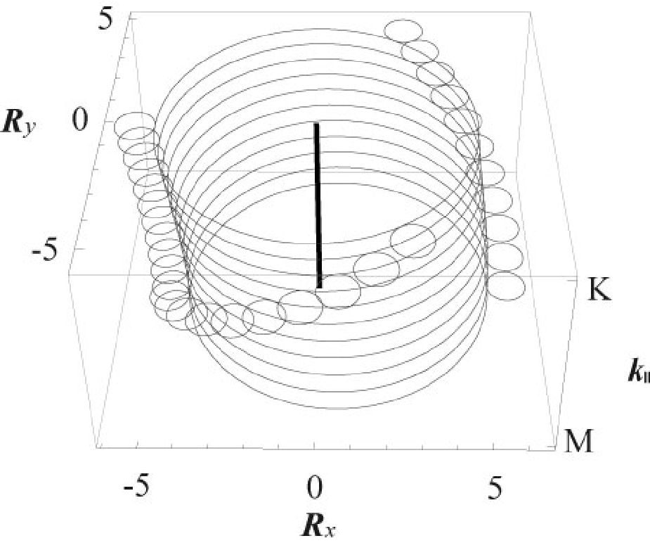
Thirdly, we can modify to zero preserving the gap open. For the arbitrary surface of Si or Ge, is zero. The condition that is restricted in a two-dimensional plane is called as a chiral symmetry[13]. The loop is given by
| (7) |
For a 2-dimensional loop, we can define a winding number as in Ref. \citenRyu_Hatsugai_2002. This is the third topological invariant we considered in the paper. The winding number is defined as the total number of times that the loop travels counterclockwise around the origin in the plane, and determines whether has edge states or not. Figure 3 shows of Ge (111) surface. In each plane vertical to the axis of Fig. 3, four loops with fixed are displayed and one of these loops encloses the origin, at each , i.e., the winding number of a link is for arbitrary , which clarifies existence of zero energy edge states. The other loops do not enclose for each , i.e., , which is consistent with absence of zero energy edge states for each . Note that zero energy edge states are doubly degenerated (left and right). This result from the winding number corresponds to the number of edge states per spin.
Finally, we modify hopping parameters except for hopping between face-to-face orbitals which locate on nearest neighbor atoms to zero adiabatically. We call this decoupled Hamiltonian as a covalent-bond model . Edge states of with the OBC corresponds to dangling bonds, where dangling bonds are defined as the covalent bonds which are cut by the surface. Of course, topological invariants and are unchanged between the adiabatic deformation. Then, implies that a covalent-bond bond exists on the link and the integer corresponds to the number of dangling bonds.
Summary of the other results
(a) Ge (110)

(b) Ge (100)

(a) Si (111)

(b) Si (110)

(c) Si (100)

Here, we summarize results of the other surfaces of Si and Ge studied in the same manner as Ge (111). As shown in Figs. 4 and 5 in addition to in Fig. 2 (b), each energy band diagram of edge states of Ge (110), Ge (100), Si (111), Si (110), and Si(100) shows different energy dependence. These edge states are all doubly degenerated due to two sides of surface. In Ge (110), Si (110), Ge (100), and Si (100), value of energy split between two kind of edge states is roughly estimated as bonding states and anti-bonding states of two dangling bonds on the surface. Especially, the edge states merged into the bulk bands for (100) cases and we cannot define the number of edge states .
The Berry phase turns out to be quantized by the anti-unitary symmetry and succeed in clarification of the three surfaces for Si, Ge, and the decoupled covalent-bond model after the adiabatic transformation while fails for the (100) surface, as summarized in Table 1. Since it is topological quantity, the result does not depend on the detail of the tight binding parameters unless the gap remains open. Then, Ge and Si with the same surface are equivalent from a viewpoint of the Berry phases.
After the adiabatic deformation described above, the winding number for the chiral symmetric Hamiltonian classifies the different surfaces. The results are also summarized in Table 1. The sign of determines whether the loop is clockwise or anti-clockwise, and becomes important to classify and surfaces. The latter is identical to surface. We note that can be defined for the chiral symmetric Hamiltonian of Ge (100) and Si (100), because edge states emerges from the bulk bands into the gap in the adiabatic transformation. However, we cannot allow such adiabatic transformation if we consider as a topological invariant.
The decoupled covalent-bond model clarifies the meaning of topological invariants because edge states are identified as dangling bonds. Then, of each materials refers the number of dangling bonds, and a non-trivial () value of indicates the link where a dangling bond exists.
| Surface | per spin | ||
|---|---|---|---|
| Si, Ge, CB (111) | |||
| Si, Ge, CB (110) | |||
| Si, Ge (100) | — | ||
| CB (100) |
Conclusion
In conclusion, we have studied topological invariants at some ideal surfaces of Ge, Si described by the tight binding model with Slater and Koster’s parameter. Following the previous study on the quantized Berry phase[9], we have defined the surface-specified Berry phase. It should be emphasized that the symmetry required for quantization of the Berry phase is the inversion and conjugate complex symmetry while it is the particle-hole symmetry and conjugate complex symmetry in the previous study. It will suggest a possibility for studies of the other materials without the particle-hole symmetry.
From the adiabatic transformation, Ge, Si, and the decoupled covalent-bond model with the same surface are topologically equivalent from a viewpoint of the Berry phase. In other words, these topological invariants successfully deduced the simple picture of dangling bonds from the complicated tight binding model with a spin-orbit coupling. Moreover, the results show that the Berry phase is successful for all surfaces of Ge, Si and provide information about a position of dangling bonds.
Finally, we comment on GaAs. For the (111) surface, there are four edge states . The value of energy split of edge bands is roughly estimated as difference between on site potential of two atoms. The site potential makes it difficult the adiabatic transformation to the simple model as is the case with Si, Ge (100). The Berry phase cannot be quantized because GaAs has no inversion symmetry. However, the Berry phase defined by another twist angle can overcome the difficulty if a anti-unitary symmetry for it’s quantization is founded in GaAs,
Acknowledgements.
We acknowledge discussions with T. Hirano. This work was supported by Grant-in-Aid from the Ministry of Education, No. 17540347 from JSSP, No.18043007 on Priority Areas from MEXT and the Sumitomo Foundation. Some of numerical calculations were carried out on Altix3700BX2 at YITP in Kyoto University.References
- [1] K. v. Klitzing, G. Dorda, and M. Pepper: Phys. Rev. Lett. 45 (1980) 494.
- [2] D. J. Thouless, M. Kohmoto, M. P. Nightingale, and M. den Nijs: Phys. Rev. Lett. 49 (1982) 405.
- [3] Y. Hatsugai: Phys. Rev. Lett. 71 (1993) 3697.
- [4] Y. Tanaka and S. Kashiwaya: Phys. Rev. Lett. 74 (1995) 3451.
- [5] S. Kashiwaya and Y. Tanaka: Phys. Rev. B 51 (1995) 1350.
- [6] M. Fujita, K. Wakabayashi, K. Nakada, and K. Kusakabe: J. Phys. Soc. Jpn. 65 1920 (1996).
- [7] S. Okada and A. Oshiyama: Phys. Rev. Lett. 87 146803 (2001).
- [8] V. Heine: Phys. Rev. 138 (1965) A1689.
- [9] Y. Hatsugai: J. Phys. Soc. Jpn. 75 (2006) 123601.
- [10] I. Maruyama and Y. Hatsugai: J. Phys. Soc. Jpn. 76 (2007) 113601.
- [11] R. D. King-Smith and D. Vanderbilt: Phys. Rev. B 47 (1993) 1651.
- [12] R. Resta: Berry’s Phase and Geometric Quantum Distance: Macroscopic Polarization and Electron Localization, Lecture notes for the ”Troisième Cycle de la Physique en Suisse Romande” (Lausanne 2000).
- [13] S. Ryu and Y. Hatsugai: Phys. Rev. Lett. 89 (2002) 077002.
- [14] W. Shockley: Phys. Rev. 56 (1939) 317.
- [15] J. Bardeen: Phys. Rev. 71 (1947) 717.
- [16] K. Takayanagi, Y. Tanishiro, M. Takahashi, and S. Takahashi: J. Vac. Sci. Technol. A, Vac. Surf. Films 3 (1985) 1502.
- [17] R. S. Becker, J. A. Golovchenko, and B. S. Swartzentruber: Phys. Rev. Lett. 54 (1985) 2678.
- [18] Y. Yamamoto, S. Ino, and T. Ichikawa: Jpn. J. Appl. Phys. 25 (1986) L331.
- [19] H. Noro and T. Ichikawa: Jpn. J. Appl. Phys. 24 (1985) 1288.
- [20] K. Inoue, Y. Morikawa, K. Terakura, and M. Nakayama: Phys. Rev. B 49 (1994) 14774.
- [21] Y. Yoshimoto, Y. Nakamura, H. Kawai, M. Tsukada, and M. Nakayama: Phys. Rev. B 61 (2000) 1965.
- [22] J. C. Slater and G. F. Koster: Phys. Rev. 94 (1954) 1498.
- [23] G. Grosso and C. Piermarocchi: Phys. Rev. B 51 (1995) 16772.
- [24] G. Klimeck, R. Bowen, T. Boykin, C. Salazar-Lazaro, T. Cwik, and A. Stoica: Superlattices and Microstructures 27 (2000) 77.
- [25] T. B. Boykin, G. Klimeck, R. C. Bowen, and F. Oyafuso: Phys. Rev. B 66 (2002) 125207.
- [26] C. Kittel: titleIntroduction to Solid State Physics Seventh Edition (Wiley, New York, 1996).
- [27] I. Ivanov, A. Mazur, and J. Pollmann: Surface Science 92 (1980) 365.