Dielectric quantification of conductivity limitations due to nanofiller size in conductive powders and nanocomposites
Abstract
Conducting submicron particles are well-suited as filler particles in non-conducting polymer matrices to obtain a conducting composite with a low percolation threshold. Going to nanometer-sized filler particles imposes a restriction to the conductivity of the composite, due to the reduction of the density of states involved in the hopping process between the particles, compared to its value within the crystallites. We show how those microscopic parameters that govern the charge-transport processes across many decades of length scales, can accurately and consistently be determined by a range of dielectric-spectroscopy techniques from a few Hz to infrared frequencies. The method, which is suited for a variety of systems with restricted geometries, is applied to densely packed 7-nm-sized tin-oxide crystalline particles with various degree of antimony doping and the quantitative results unambiguously show the role of the nanocrystal charging energy in limiting the hopping process.
pacs
73.22.-f, 72.80.Tm, 73.63.Bd, 77.84.LfI Introduction
Small submicron particles are well-suited as fillers in non-conducting polymer matrices to obtain a conducting composite with a percolation threshold (far) below 1 %. The low percolation threshold is due to the formation of airy aggregates of conducting particles, in which the particles are grown together by diffusion-limited cluster aggregation, creating a network with a fractal dimension around 1.7. [1, 2, 3] These airy aggregates can be thought of as conducting spheres forming a 3-dimensional percolating network around the expected aggregate filling fraction 0.16. As a consequence of the fractal structure within the aggregates, the filler fraction of the particles at the percolation point is much lower. Even in case the particles touch, the dc conductivity () of these composites at high filling fractions turns out to be orders of magnitude lower than of the bulk material, as was recently illustrated for a particular crosslinked epoxy composite with filler particles of Phthalcon-11, [4] Co phthalocyanine crystallites of 100 nm size, and explained by purely structural arguments.[5]
When crystalline particles with a diameter of less than 10 nm instead of 100 nm are used, the small size of the particles may impose another important restriction to the maximal possible composite conductivity, which is due to the density of states (DOS) involved in the dc conductivity through the network of particle contacts. Compared to larger crystallites, this DOS can be strongly reduced by the charging energy.[6, 7, 8, 9]
We show how those microscopic parameters, which govern the charge-transport process across many decades of length scales, can accurately and consistently be determined by ac (alternating current) dielectric spectroscopy from a few Hz to infrared frequencies. In particular we can address the parameters for Mott variable-range hopping, for heterogeneity-induced enhanced ac response, for phonon- or photon-assisted nearest-neighbor hopping, and for the Drude response of individual nanocrystals. Due to these quantitative results we can unambiguously determine also the role of the nanocrystal charging energy in limiting the hopping process. We apply the method to antimony-doped tin-oxide (ATO) crystallites of 7 nm diameter and to 100 nm sized crystallites of Phthalcon-11. It turns out that in densely packed crystallites of ATO, due to the strong influence of the charging energy on the DOS, at room temperature is four orders of magnitude lower than the dc conductivity extrapolated from the Drude plasma frequency () of the crystallites - a result with obvious implications for the design of conducting composites. The dielectric method is well suited for a variety of systems with restricted geometries, as we will illustrate by a short discussion of phase-change materials [10] and granular oxides. [11].
II Conductivity in conducting polymer composites and granular metals
For randomly placed conducting spheres in an insulating matrix, the relation between and the fraction of spheres is known from percolation theory. [12, 1, 13]Above the percolation threshold where is the percolation threshold, and is approximately equal to the conductivity of the spheres. [14, 3] When the building blocks of the network are fractal aggregates instead of solid spheres, has to be replaced by the aggregate conductivity and depends on the particle conductivity and, via the non-linear relation with , on the real percolation threshold of the particles.[5] The value of the exponent is related to the random-walk dimension and the fractal dimension , and is maximally . This shows that on purely geometrical grounds for a network with , at the highest filling fraction of the aggregates will be three to four orders of magnitude lower than in the pure filler powder. [5]
As remarked in the introduction, when nanosized particles are used as fillers, charging energies (and quantum size effects) impose a further important restriction to the maximal possible composite conductivity.[6, 7] This effect can be conveniently studied in densely packed powders of filler material by dielectric spectroscopy.
II.1 Parameters for the dc conductivity
In the ohmic regime, if there is a non-negligible density of states around the chemical potential, and the temperature is high enough that also the Coulomb interaction can be neglected (), will obey Mott’s equation for conduction via variable-range hopping (VRH): [15]
| (1) |
with and
| (2) |
where denotes the decay length of the electron density, the Boltzmann constant, and the density of states relevant in the hopping process. [16]
For randomly packed spheres of radius and spacing the localization length will be enlarged, [17, 18, 7, 8, 9] and can be approximated by [17, 7]
| (3) |
In the following we drop the tilde.
Below the dependence of the conductivity will be dominated by a soft Coulomb gap, leading to so-called Efros-Shklovskii (ES) VRH: [19]
| (4) |
In the ES VRH model in the dilute limit of a large distance between the particles is given by
| (5) |
with the electron charge, the vacuum dielectric constant, and the relative dielectric constant of the medium. is given by and (for ) the charging energy by .
For densely packed small particles, at high temperatures but still in the regime, where Coulomb interactions are important (), ES VRH behavior will evolve into nearest-neighbor hopping at a temperature . Above the conduction is thermally activated with an activation energy of the order of the charging energy, and .
II.2 Sub-THz and far-infrared regime
At sufficiently low frequencies the conductivity will be frequency independent and equal to its dc value, because the inhomogeneities are averaged out by the motion of the charge carriers. The minimal length scale for homogeneity is referred to as ,
| (6) |
where is the density of the carriers involved in the hopping process at the border of the homogenous regime, and the onset frequency for the frequency dependence of is divided by , with the dimension of the system. [16]
At high enough frequencies, when during half a period of the oscillation of the applied field electrons can hop solely between nearest-neighbors, the major contribution to the conductivity will be due to tunnelling between localized states at neighboring sites (the pair limit).[22] This incoherent process can be either by phonon-assisted or photon-assisted hopping, where in the latter case the energy difference between the sites is supplied by photons instead of phonons. [16] The phonon-assisted contribution to the conductivity is given by
| (7) |
with the decay length of the electronic state outside the conducting particles, the relevant DOS at the Fermi energy , and the phonon ‘attempt’ frequency.[16] This formula is valid when ; at higher , where the contribution of phonon-assisted hopping to becomes constant, photon-assisted processes usually take over, with a conductivity given by
| (8) |
The energy in eq. (7) is in eq. (8) replaced by and the phonon attempt frequency by , with being the ‘overlap’ pre-factor for the energy levels of two neighboring sites. In analogy with , can be interpreted as the attempt frequency for photon-assisted hopping. Equation (8) is only valid when . As in phonon-assisted hopping, passes over into a plateau at high .
II.3 Visible and optical response
At high frequencies (for ATO in the infrared regime) the short period of the electromagnetic field will restrict the motion of the carriers to the nanocrystallite, and the dielectric response characterized by the complex relative dielectric constant will be Drude-like, with the Drude plasma resonance frequency and the damping rate. In practice the constant 1 has to be replaced by due to other contributions in this frequency regime, like the polarization of the ion cores. [23] The Drude plasma frequency is related to the number of carriers per unit of volume and the effective mass as
| (9) |
For damping rates comparable to the Drude plasma frequency, the real plasma frequency (where the dielectric constant becomes zero) will be larger than . is determined by the boundaries of the nanoparticle and additional (ionized impurity) scattering:
| (10) |
where is the sum of the inverse size of the particle and the inverse phonon scattering length.
III Experimental procedures and data
Measurements were performed on Sb-doped tin-oxide nanoparticles with [Sb]/([Sn]+[Sb]) equal to 0, 2, 5, 7, 9, and 13 at.%. The particles are monocrystalline and spherical with diameters close to 7 nm. [24] The diameter of the 7% doped crystallite is 7.1 nm. Sb is incorporated in the casserite SnO2 lattice by replacing Sn4+. At the doping level of 7%, Sb is mainly present as Sb5+, resulting in n-type conductivity of the ATO particles according to Nutz et al.. [25] The amount of Sb3+ present in the particles is negligibly small. [24, 26]
The followed experimental procedures for the dc conductivity and dielectric measurements are described in Refs. 5 and 27. The thickness of the samples was typically a few mm. The dc conductivity measurements were performed in the dark under helium atmosphere.
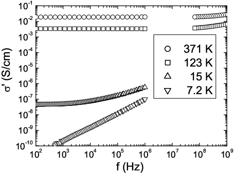
The dependence is given in Fig. 1, and the frequency dependence at temperatures down to 7 K in Fig. 2. All data shown are for 7%-doped ATO. Similar results were obtained at other doping levels, be it with different absolute values. The data were taken in the ohmic regime.

| sample | N | ||||
|---|---|---|---|---|---|
| (cm-3) | (S/cm) | (s-1) | (s-1) | () | |
| ATO-film[28] | 0.3 | ||||
| ITO-film[29] | 0.35 | ||||
| ATO-powder[25] | 0.27 | ||||
| ATO-powder(pw) | 0.3 |
The infrared (IR) transmittance was measured on a pellet of KBr mixed with a small amount of ATO. For the IR-reflectance we used a precipitated film of ATO with a thickness of about 1 mm. The data are shown in Fig. 3. For the analysis we also used the sub-THz transmittance and phase data (only shown in Fig. 4).

In Table 1 we summarize our data on densely packed 7-nm-sized ATO crystallites and compare them with measurements on doped tin oxide published in the literature. The values of agree within a factor 2, while the spread in the scattering rates is larger.
IV Analysis and Discussion
In the analysis we first show the procedure to extract the parameter values from the data in the different frequency regimes and to check their consistency. We also make a comparison to the parameter values of Phthalcon-11, for which the data are published elsewhere. [27] Then we concentrate on the density of states; the latter being important for the dc conductivity. Subsequently, the implications for the use of the particles as fillers in nanocomposites are discussed.
IV.1 Procedure
Regarding the dependence of (Fig. 1), the data can be fitted with (eq. (1)) if the fit is restricted to K and with (eq. (4)) for K. The fit gives an activation energy of K, while the exponent at low gives K. The localization length from , see eq. (5), is calculated to be = 3 nm. Using eq. (3) and estimated from the packing density, we find nm, in good agreement with the value calculated from .
The onset of the frequency dependence of the conductivity (see Fig. 2) signals that the carrier starts to feel the inhomogeneity of the underlying structure. Using eq. (7), the typical length scale at the onset can be found. For 7%-doped ATO at 300 K, the onset frequency Hz and S/cm give a value of cm-1.
The linear frequency dependence of the conductivity at 7 K in the double logarithmic plot of Fig. 2, is in agreement with phonon-assisted tunneling, see eq. (7). In the range of 10 - 100 cm-1 photon-assisted processes take over.[30] Applying eq. (7) to the conductivity data at 293 K and taking the usual value for the phonon frequency in solids s-1,[16, 30] we find eV-2cm-1, see Fig. 4.
Turning next to the high-frequency data presented in Fig. 3, we performed a simple Drude analysis. The fit ( = 11000 cm-1 and = 3300 cm-1, together with a dielectric constant of 4.0) reproduces the main features of the increase of the transmission and the level of the reflectance (the oscillations in the fit to the transmittance are an artefact because the effective ATO film thickness of 0.005 mm is much smaller than the real thickness of the pressed KBr pellet). The number of carriers of cm-3 is directly derived from the Drude frequency and is slightly lower than obtained from a simple interpretation of the chemical composition. The bulk dc conductivity calculated from the Drude parameters is S/cm. The fit parameters of the present samples are given in Table 1 and agree well with the literature.
Fig. 4 shows the reconstructed conductivity of ATO as function of frequency due to the processes discussed above.

For ATO the important values for the dc conductivity can be deduced from the combination of variables that we found from the previous analysis (i) cm-1, (ii) J-2m-1 or for photon-assisted hopping and J-2m-1 for the phonon-fit to the data at 7 K, and (iii) cm-3 and s.
Using (iii) the ‘extrapolated’ dc conductivity is S/cm, a factor larger than the found value of S/cm. The estimated Fermi energy is around 2 eV, and from (valid for free electrons) we get eV-1cm-3. From (ii) with of 3 nm, we find for eV-1cm-3, a factor lower than . Note that this is an averaged density of states involved in photon assisted hopping. Due to the curvature of the density of states around the chemical potential, will be lower at lower energies. For example, for the phonon-fit at 7 K is equal to eV-1cm-3.
The values for and can be used as a consistency check. The combination of the estimated Fermi velocity of cm/s, with the crystallite size of 7 nm and ,[25] predicts a surface scattering rate of s-1, in agreement with the found value of . Next, from eV-1cm-3 we now can estimate at K as cm-3. Using (i) and we find 0.3 m.
In short, the dielectric data of ATO allow a consistent picture of the conduction process. In these densely packed crystallites the localization length is enhanced by a factor 10 and the density of states involved in the dc conductivity is more than a factor smaller than that in the conduction within the crystallites. The relatively large length scale for homogeneity is indicative for the presence of aggregates. Indeed, like in Ketjen-Black, [2] nanoparticles of ATO are known to form chemically bonded aggregates that survive the preparation stage.[24] Due to the nature of the chemical bond, the conductivities between neighboring crystallites in and outside the aggregates are expected to be only slightly different. Note that also the value of has to be seen as an average, as inhomogeneities in the doping of ATO might be present as well.[26, 24]
For the studied Phthalcon-11 crystallites s-1 and s leading to cm-3, i.e. about 1 charge per crystallite.[27] The other values found for Phthalcon-11 are: (i) cm-1, (ii) J-2m-1 or . In these organic crystals with such a low carrier density, the charge carriers can be seen as an electron gas with an energy scale set by , and can be estimated from to be . This value of is the upper limit for and . From , we find a decay length of 3 nm, as expected from the packing.
The Phthalcon-11 parameters show that the crystals are semiconducting crystals with a low number of charge carriers. All charges participating in the conductivity within the crystal also contribute to the dc conductivity. As for ATO the obtained conduction parameters for Phthalcon-11 from the dielectric scans give a consistent picture.
IV.2 Density of states
For ATO, the differences between the density of states involved in the hopping process eV-1cm-3 and the Drude conduction within the crystallites eV-1cm-3 are clearly significant. The result is as anticipated from the estimated charging energy of the order of 50 meV, and shows its importance for the dc powder conductivity.
For Phthalcon-11 the very low number of carriers involved in the hopping process is similar to the number of carriers that determines the Drude contribution in the crystallites. Since the mean size of the particles is 20 times larger than for ATO, the charging energies will be of the order of 3 meV, and hence are expected to be negligible at room temperature.
IV.3 Implications
In polymer nanocomposites with building blocks formed by diffusion-limited cluster aggregation, the airy structure of the particle network gives a strong reduction in conductivity of the composite compared to the filler (for the Phthalcon11/polymer composite a factor ). [5] This effect can be compensated by using better conducting particles. Particles of ATO or ITO seem to be well-suited as the material is known to be very well-conducting. In addition, ATO crystallites are relatively easily obtained in sizes around 7 nm, and ‘when properly dispersed can give polymer composites with a low percolation threshold.[31] However, even if the filler nanoparticles in the composite touch, they will not be in better contact than in a densely packed powder. As shown here for ATO, for these small crystallites the DOS involved in is dramatically reduced due to the shift of the energy levels away from the Fermi level by Coulomb charging effects. As a consequence, an additional four orders of magnitude in are lost compared to the bulk value.
Other systems where size restrictions are expected to be present might be conveniently studied in a similar way. For example several chalcogenide alloys exhibit a pronounced contrast between the optical absorption in the metastable rocksalt after the intense laser pulse and in the initial amorphous phase. [10] As shown by extended x-ray absorption fine structure spectroscopy (EXAFS) the resistive change after the intense laser recording pulse goes together with a crystallization process, where also small domains are inherently present. Our dielectric method might visualize to what extent the domain walls after crystallization limit the conductivity and have consequences for the band structure calculations. If the walls become real barriers quantum size effects in the small domains will invalidate the use of periodic boundary conditions in the calculations. Also the glassy behavior in the conductance of deposited indium-tin oxide samples in the insulating regime, [11] and of quench-condensed insulating granular metals [32] might be further clarified by the use of our dielectric approach and analysis. Scanning the frequency will reveal the evolution of the length scales and DOS involved in the relaxation processes.
V Conclusions
By combining data of sub-THz transmission with infrared transmission and reflection we were able to explain the full frequency response of densely-packed nanosized crystallites using the parameters for Mott variable-range hopping, for heterogeneity-induced enhanced ac response, for phonon- or photon-assisted nearest-neighbor hopping, and for the Drude response of individual nanocrystals. For 7 nm antimony-doped tin-oxide particles the analysis unambiguously quantified the reduction of the density of states involved in the dc conduction compared to the value extrapolated from the Drude response at infrared frequencies. Dielectric scans with a similar analysis will also be revealing in other systems where size limitations are expected to play a role.
Acknowledgements.
It is a pleasure to acknowledge Roel van de Belt of Nano Specials (Geleen, The Netherlands), who made the ATO samples available, and Matthias Wuttig from the Physikalisches Institut of the RWTH Aachen University in Germany for fruitful discussions about phase-change materials. This work forms part of the research program of the Dutch Polymer Institute (DPI), project DPI435.References
- [1] Fractals and Disordered Systems, eds. A. Bunde and S. Havlin (Springer-Verlag, Berlin, 1991).
- [2] D. van der Putten, J. T. Moonen, H. B. Brom, J. C. M. Brokken-Zijp, and M. A. J. Michels, Phys. Rev. Lett. 69, 494 (1992); L. J. Adriaanse, J. A. Reedijk, P. A. A. Teunissen, H. B. Brom, M. A. J. Michels, and J. C. M. Brokken-Zijp, Phys. Rev. Lett. 78, 1755 (1997).
- [3] C. Grimaldi, T. Maeder, P. Ryser, and S. Strässler, Phys. Rev. B 68, 024207 (2003); C. Grimaldi and I. Balberg, Phys. Rev. Lett. 96, 066602 (2006).
- [4] J. C. M. Brokken-Zijp, D. P. de Bruijn, K. P. Datema, C. A. Emeis, A. H. Kramer, J. B. van Mechelen, and A. J. Meruma, patents: US05319009, EP0064254A1, WO09324562A1.
- [5] L. J. Huijbregts, H. B. Brom, J. C. M. Brokken-Zijp, M. Kemerink, Z. Chen, M. de Goeje, M. Yuan, and M. A. J. Michels, J. Phys. Chem. B 110, 23115 (2006).
- [6] D. Yu, C. Wang, B. L. Wehrenberg, and P. Guyot-Sionnest, Phys. Rev. Lett. 92, 216802 (2004).
- [7] J. Zhang and B. I. Shklovskii, Phys. Rev. B 70, 115317 (2004).
- [8] I. S. Beloborodov, A. V. Lopatin, and V. M. Vinokur, Phys. Rev. B 72, 125121 (2005).
- [9] M. V. Feigelman and A. S. Ioselevich, JETP Lett. 81, 277 (2005).
- [10] W. Welnic, S. Botti, L. Reining, and M. Wuttig, Phys. Rev. Lett. 98, 236403 (2007); M. Wuttig and N. Yamada, Nature materials 6, 824 (2007).
- [11] M. Ben-Chorin, Z. Ovadyahu, and M. Pollak, Phys. Rev. B 48, 15025 (1993); A. Vaknin, Z. Ovadyahu, and M. Pollak, Phys. Rev. Lett. 84, 3402 (2000); V. Orlyanchik and Z. Ovadyahu, Phys. Rev. B 75, 174205 (2007).
- [12] D. Stauffer and A. Aharony, Introduction to percolation theory (Taylor & Francis, London, 1985).
- [13] J. P. Straley, J. Phys. C 9, 783 (1976), Phys. Rev. B 15, 5733 (1977).
- [14] R. Zallen, The Physics of Amorphous Solids (Wiley and Sons, New York, 1983).
- [15] N. F. Mott, Philos. Mag. 19, 835 (1969).
- [16] H. Böttger and V. V. Bryksin, Hopping Conduction in Solids (Akademie-Verlag, Berlin, 1985).
- [17] R. Németh and B. Mühlschlegel, Z. Phys. B 70, 159 (1988).
- [18] I. P. Zvyagin, JETP Lett. 69, 932 (1999).
- [19] B. I. Shklovskii and A.L. Efros, Electronic Properties of Doped Semiconductors (Springer-Verlag, Berlin, 1984).
- [20] The energy levels are discrete and assumed to have an overall homogeneous linewidth around 100 meV.
- [21] Due to a different geometry, the activation energies in the deposited films of CdSe nanoparticles found by I. Balberg et al., Phys. Rev. B 75, 153301 (2007), are larger.
- [22] M. Pollak and T. M. Geballe, Phys. Rev. 122, 1742 (1961).
- [23] C. Kittel, Introduction to Solid State Physics (John Wiley and Sons, New York, 7th edition 1996).
- [24] W. E. Kleinjan, J. C. M. Brokken-Zijp, R. van de Belt, Z. Chen, and G. de With, J. Mater. Res., accepted.
- [25] T. Nütz, U. zum Felde, and F. Haase, J. Chem. Phys. 110, 12142 (1999).
- [26] C. McGinley, H. Borchert, M. Pflughoefft, S. Al Moussalami, A. R. B. de Castro, M. Haase, H. Weller, and T. Möller, Phys. Rev. B 64, 245312 (2001).
- [27] L. J. Huijbregts, H. B. Brom, J. C. M. Brokken-Zijp, M. A. J. Michels, M. de Goeje, and M. Yuan, Phys. Stat. Sol.(c) 3, 259 (2006); L. J. Huijbregts, H. B. Brom, J. C. M. Brokken-Zijp, M. Yuan, and M. A. J. Michels, Phys. Stat. Sol. (c), accepted.
- [28] E. Shanthi, V. Dutta, A. Banerjee, and K. L. Chopra, J. Appl. Phys. 51, 6243 (1980).
- [29] D. Mergel and Z. Qiao, J. Phys. D:Appl. Phys. 35, 794 (2002).
- [30] J. A. Reedijk, L. J. Adriaanse, H. B. Brom, L. J. de Jongh, and G. Schmid, Phys. Rev. B 57, R15116 (1998); J. A. Reedijk, H. C. F. Martens, H. B. Brom, and M. A. J. Michels, Phys. Rev. Lett. 83, 3904 (1999).
- [31] V. A. Soloukhin, J. C. M. Brokken-Zijp, and G. de With, J. Pol. Sci. B 45, 2147 (2007).
- [32] N. Kurzweil and A. Frydman, Phys. Rev. B 75, 020202(R) (2007).