Constructing Spin Interference Devices from Nanometric Rings
Abstract
The study of nanospintronic devices utilizing coherent transport through molecular scale multiply-connected geometries in the presence of moderate magnetic fields is presented. It is shown how two types of simple devices, spin filters and spin splitters (or Stern-Gerlach devices) may be constructed from molecular nanometric rings utilizing the Aharonov-Bohm effect. The current is calculated within a single electron approximation and within a many-body master equation approach where charging effects are accounted for in the Coulomb Blockade regime. We provide rules and tools to develop and analyze efficient spintronic devices based on nanometric interferometers.
I introduction
In recent years a great deal of attention has been devoted to the study of useful electronic devices utilizing the Aharonov-Bohm Aharonov1959 (AB) phase in multiply-connected geometries.Webb85; Timp87; Yacoby95; Oudenaarden98; Fuhrer01; Smalley04; Ensslin05 In particular, there has been interest in spin-sensitive devices Takayanagi99; Richter01 that are the single-electron analogue of semiconductor spintronics.Malajovich2001 Most of the research conducted in this direction has focused on mesoscopic systems, where the AB flux quantum matches weak magnetic fields, inter-electronic dependencies can be relatively negligible, and the Rashba Rashba60 and Dresselhaus Dresselhaus55 spin-orbit coupling or inhomogeneous magnetic fields,Richter04a; Richter04b provide a large and controllable dependency of the electron Hamiltonian on directionally significant spin eigenvalues.Richter01; Klapwijk02; D'Amico03; Richter04c; Vasilopoulos04; Sigrist05; Vasilopoulos05; Peeters06; Perroni06
At the nanometric scale, it has been shown that spin-independent AB molecular interferometers may be possible at reasonable magnetic fields when the coupling of the device to the leads is small.Hod2004; Hod2005a; Hod2005b; Hod2006a For such small AB interferometers there are striking differences in the properties of magnetic versus electric gauges, and the magnetic gate becomes advantageous over electrical gating.Hod2005b; Hod2006b For example, the current in a multi-terminal molecular device can be tuned by changing the polarity of the magnetic field utilizing its symmetry breaking nature.Hod2005b Another example includes fundamental differences between magnetic and electric gates with respect to inelastic effects.Hod2006b
Previous studies of nanometeric molecular AB interferometers have ignored the spin degree of freedom. In such molecular-scale systems, if the likes of atomic spin-orbit coupling and magnetic ions are not prevalent,Gefen89; Gefen92 the lack of a Rashba/Dresselhaus field and the difficulties in locally manipulating the external magnetic field at such scales leaves only the much smaller Zeeman term to differentiate between spins.Richter03 In addition, the small size of such devices further complicates matters by introducing large charging effects.Elhassid00 These should become especially noticeable when the coupling between the device and the leads is weak (as required for nanometeric devices operating at reasonable magnetic fields), since electrons spend a longer time on the device. Despite these inconveniences, one may very well wonder whether it is possible to develop molecular AB interferometers as single-electron spin-devices such as a spin filter or splitter. This is the question that interests us here.
In this paper we develop the basic physical foundation to develop such devices. In Section II we describe the types of devices we wish to model and define their efficiency in terms of the spin-dependent current. This includes a two-terminal spin filter and a three-terminal spin splitter. In Section III Zeeman splitting is introduced into the two models developed by Hod et al. Hod2004; Hod2005b; Hod2006a for independent spinless electrons - a simple continuum one-dimensional model and a more detailed tight-binding model. Within the simple continuum model we provide an exact solution for the spin-dependent conductivity for the two- and three-terminal devices. The role of the different model parameters is studied and comparison between the simple continuum model and the tight-binding results are made. In Section IV the tight-binding levels are used in a master equation calculation Beenakker91; Kinaret92; Bonet02; Hettler03; Datta2004; Elste05; Braig05; Mukamel06; Hanggi2006; Nitzan07 to examine charging effects in the Coulomb blockade regime. From this basic analysis some interesting conclusions are drawn regarding the properties and limitations of nanospintronic AB devices, and a few potential avenues for further research are pointed out in Section V.
II Devices

We will examine two types of elementary nanometric devices with and without charging effects: a spin filter and a spin splitter, as illustrated in Fig. 1. Such devices might be built from molecular rings such as the polycyclic aromatic hydrocarbon,Hod2005a; Staab1978; Hajgato2004 or from atomic corrals (with the advantage of controlled structure and electron density).Collins1993; Manoharan00 Such corrals can be constructed atom by atom using scanning tunneling microscopy techniques.Ho03 A more exotic example involves 3D nanostructures such as torus knots, where a periodicity of more than can be achieved, producing a stronger AB effect than simple rings. In such molecular structures, control over the structure’s geometry is possible at the atomic level (unlike the case of mesoscopic rings).
The filter does not really require something as complex as an AB ring for its realization. One only requires two single-spin levels which can, by manipulation of the magnetic field, be moved in and out of the conduction energy window, and any atom, quantum dot, or other discrete system can meet this requirement. This case is treated because it provides a simple example with only two terminals and yet may still be useful. The splitter is a molecular Stern-Gerlach device and is somewhat more interesting: having three terminals, it actually requires a device which, like an AB ring, has some sort of inherent asymmetry in either its construction or in the spinor wavefunction.
It is useful at this point to examine the energy scales of the problem. The Fermi energy is the most important parameter. For a half-filled conduction band the Fermi wavelength is of the order of four bond lengths . This gives a Fermi energy of if we set the lowest level to zero, regardless of ring size and assuming atomic spacing of about . To a good approximation, the molecular orbital energy (at zero magnetic field ) is given by an effective mass model , where , is the radius of the ring and is the effective mass. This gives a value for the Fermi quantum number of . Electronic levels on the rings near the Fermi energy are separated by , which reduces linearly with . For rings of the order of several nanometers in diameter the separation between levels near the Fermi energy is of the order of sub electron volts. This is also the order of magnitude of the charging energies . Other energy scales involve the magnetic field splitting which can be as large as the level spacing and the Zeeman splitting per Tesla, which is only about a third of the thermal energy at .
The effectiveness of these devices can be judged not only by output polarization, but also by unitarity: a perfect device always sends the correct electrons into the correct lead. More precisely, the two devices that will be discussed are judged by the following quantities:
| (1a) | |||
| (1b) | |||
| (1c) | |||
Here is the up/down current for the two terminal device and is the up/down current for channel or for the three terminal device. The only important properties these quantities need to have for the purpose of this work is that they should be bounded from above by , and should reach only in the case of perfect operation. For the two and three terminal devices both requirements are satisfied. We refer to them from now on as “efficiencies”.
The problem of building a perfect device can thus be mathematically restated as the problem of optimizing its efficiency to the desired value, usually unity, over the space of all controllable parameters. These include the magnetic field, the ring’s radius and structure, the gate and bias voltage (or the chemical potential) and the lead placement and coupling. Reasonable ranges for these parameters must be assumed: magnetic fields of more than a few Tesla may pose a technical limitation, as are large rings where disorder effects begin to dominate.Aronov1987 The leads cannot be too close to one another to avoid direct tunneling and should be coupled strongly enough to make the environmental coupling unimportant. Even within these limits, the problem remains numerically formidable in all models. We will therefore also discuss a conceptually simpler if less systematic way of designing perfect devices.
III Single Electron Picture
In this section we describe the physical principles required to construct molecular spin filter and spin splitter devices in the limit where charging effects can be ignored and the complexity of the many-body physics can be reduced to a simplified one-electron picture.
III.1 Basic Concepts
To discuss the basic physical principles involved, let us first regard a simple analytical model for the transmission through an AB ring.Richter01; Richter04a; Richter04b; Richter04c; Peeters06 The physics of this model for molecular conductors was recently discussed by Hod et al. in the absence of Zeeman splitting and spin-orbit coupling.Hod2004; Hod2005a; Hod2005b; Hod2006a Consider a one dimensional AB interferometer as shown in Fig. 1. It consists of a conducting ring of radius coupled to two or three conducting wires placed in a perpendicular uniform magnetic field, . The device is described by the Pauli Hamiltonian:
| (2) |
where , is the vector potential (), is the electrostatic potential on the ring, and is the electron mass. The last term in Eq. (2) represents the coupling of the magnetic field to the spin angular momentum, where are the Pauli matrices, is the gyromagnetic ratio (we take for the spin), and is the electron Bohr magneton. The lack of a Rashba field in molecular conductors allows us to safely ignore spin-orbit coupling effects. In the common case where the scalar potential governing the system is periodic or nearly so, the effective mass approximation can be used and the Pauli Hamiltonian can be reduced to:
| (3) |
where is the effective mass of the electrons. Since the two additive terms in the Hamiltonian must commute (one depending only on the orbital part and the other on the spin part of the wavefunction), we can adopt the solution of Hod et al. Hod2004; Hod2005b for the transmission of electrons through the two prototype devices (spin filter and splitter). We adopt a transformation which allows us to project spin effects onto a calculation where spin was previously neglected, noting that the spin dependent part of the Hamiltonian under a constant field must have the two eigenvalues for spin up/down electrons. This transformation is not limited to the specific Hamiltonian described above: the only requirement is that does not contain a spin dependency. Furthermore, even for inhomogeneous magnetic fields, where the spin-dependent term in the Hamiltonian does not commute with , a similar transformation in the limit of adiabatic spin dynamics can be made, where in addition to a shift in energy one has to introduce a shift in the magnetic flux.Richter01a
Using the standard analytical approach of treating a 1D ring based on a scattering matrix formalism,Gefen84 the transmission as a function of energy, previously calculated for spinless electrons,Hod2004; Hod2005b need only be modified by the Zeeman energies for up (down) electrons, which affects only the kinetic phase angles in the expression:
| (4) |
The transmission itself is the solution of the linear scattering problems with the final results for the two-terminal device shown in the upper panel of Fig. 1 given by:
| (5) |
where is the ratio between the magnetic flux and the quantum flux , and we have defined:
| (6) |
with the transmission amplitude into the junctions and the junction scattering amplitude.Hod2004
A similar calculation can be made for the more cumbersome case of a three terminal device shown in the lower panel of Fig. 1. We focus on the case where all three junctions have identical scattering amplitudes. The transmittance for channels and is given by the ratio . The denominator of the transmittance probability for both output channels is given by
| (7) |
The numerator of the transmittance probability through output channel is given by
| (8) |
and the numerator of the transmittance probability through output channel is given by
| (9) |
In the above equations , and are the angles between all three leads as defined in Fig. 1.
The current is related to the transmittance through the Landauer formula.Landauer1957 For the two terminal device the current is given by
| (10) |
where are the chemical potentials of the input/output channels and the Fermi function is . For the three terminal device the current is given by
| (11) |
where is the chemical potential for output channel or , respectively. Conductance can be obtained from the current by taking the derivative with respect to the bias voltage.
III.2 Spin Filters
We now turn to discuss the application of the above results to the construction of a spin filter device. While for the case where the Zeeman effect was neglected Hod2004; Hod2005a; Hod2006a it was always desirable to vary the gate voltage so as to shift the conduction peaks near zero magnetic field, in Zeeman spin devices this heuristic is complicated by the dependence of the splitting on the magnetic field strength. In practice, a compromise between realistically low magnetic fields and usable energy shifts restricts the sought after set of parameters. These include the kinetic phase angle and the transmission amplitude into the junction (cf., Eqs. (5) and (6)). Note that the kinetic phase angle depends on the magnetic phase angle . This is precisely where the aforementioned complication enters.
With the above convenient expressions one can calculate the spin-dependent and spin-independent conduction for different ring configurations and external parameters. Typical results are shown in Fig. 2 for zero bias voltage and for . As expected, the spin-independent conduction is periodic with a period that is equal to . Therefore, we plot only the first period, namely . We find that within each period the spin-independent conduction has a symmetric structure around , characterized by a double peak.Hod2004; Hod2006a This structure is caused by resonance transmission through the energy levels of the ring. The spin-dependent conduction follows closely the behavior of the total conduction. The up/down conduction peaks are separated by the Zeeman splittings which increase with increasing magnetic flux.
Similar to the case of spinless electrons,Hod2004 changing the coupling strength between the leads and the ring, modeled here by , changes the width of the peaks as shown in the left panels of Fig. 2. The effects of changing the kinetic phase angle are more involved than the case studied before.Hod2004 In the case of spinless electrons, the kinetic phase angle depends only on the product . Therefore, changing the energy of the conduction electron by the application of a gate voltage, changing the ring dimensions, and changing the effective mass of the conduction electron can be mapped onto a universal curve.Hod2004; Hod2006a In the present study there are three independent parameters that affect the kinetic phase angle in different ways. For example, the position of the conduction peaks can be shifted by adjusting the energy of the conduction electron by the application of a gate voltage. This is depicted in the lower left panel of Fig. 2. However, the change in the energy of the conduction electron also affects the splitting between the conduction peaks of the up/down spins as previously discussed. Altering the effective mass within the ring with the chemical potential held constant, for instance by a change of composition or inter-atomic distance in the ring atoms, modifies the kinetic phase and can thus increase or decrease the splitting as shown in the upper right panel of Fig. 2. Finally, as the ring radius is increased, the splitting for a set flux ratio decreases since this ratio then represents a smaller field as depicted in the lower right panel of Fig. 2. However, for the same reason, greater magnetic flux ratios become accessible for larger rings.
It is often more instructive to look at the results shown in the right panel of Fig. 2, where the familiar diamond-shaped conduction pattern within the energy/phase ratio plane behaves more simply and predictably, in order to gain a better intuitive understanding of the system. Here, the two ends of the white conduction lines represent up/down conduction where the chemical potential and magnetic field are at the middle of such lines. Varying still affects only the peak widths, modifying changes the lengths of the conduction lines, changing scales the diagram in the energy axis without changing the length of the conduction lines and altering the energy of the conduction electron scales the diagram along with the lines in the same axis. Thus, in order to construct an efficient spin filter one has to construct this diagram and control the position of the white conduction lines by the application of a proper magnetic field and gate voltages to achieve a desired behavior.
Good molecular spin filters can be made when two conduction peaks with different spins are sufficiently separated in energy and magnetic field to allow only electrons of one spin to traverse the ring. This is best achieved for molecular devices with a large effective mass for the conduction electron and small couplings between the leads and the ring (“bad contact”). In Fig. 3 we plot the magneto-conduction for a molecular device with relatively high effectiveness. We zoom on the region of the first magnetoconductance peak. The upper panel shows the results for a analytical model discussed above and the lower panel shows the results of an atomistic calculation for a molecular AB interferometer as illustrate in the upper panel of Fig. 1. As clearly can be seen, depending on the value of the magnetic gate, one can open output channel for spin up or down while at the same time close this channel for the other spin.
To calculate the magneto-conductance of a molecular AB interferometer we have used a simple tight-binding model where we assume a single electron in a spherical -level for each site on the molecular ring. We add the proper magnetic terms to the tight-binding Hamiltonian of the system:
| (12) |
where is the angular momentum operator, is the magnetic field vector, and the projection of onto the plane perpendicular to . A gauge invariant basis is used to evaluate the tight-binding Hamiltonian matrix: , where is a type orbital centered on site , and is the vector potential evaluated at the position of site . We take the diagonal matrix elements of to be equal to zero (energy scale) and the off-diagonal elements are proportional to the overlap between the gauge invariant basis on the different electron sites, as described in more detail in Refs. Hod2004 and Hod2006a.
The conductance is calculated using the Landauer formalism Landauer1957 which relates it to the scattering transmittance probability through the system. The transmittance is given by . Here, is the retarded Green function, is the overlap matrix, and are the imaginary parts of the self-energy () of the input/output channels. For the results presented in Fig. 3 we use both imaginary absorbing potentials Hod2004; Baer2003 and an iterative semi-infinite bulk Green functions calculation scheme Hod2005a; Lopez1984; Lopez1985; Nardelli1999 to calculate the self-energies of the leads.
Comparing the results of the simple analytical model to the results obtained from the tight-binding model indicates that the same physical picture emerges for the tight-binding approach. This is expected based on previous studies where the Zeeman effect was neglected.Hod2004; Hod2005a; Hod2006a The agreement between the two approaches indicates that the diffraction pattern is insensitive to the perturbations caused by an ionic potential and the results will not be invalidated by a more thorough (single-particle) treatment. The only free parameter used in the analytical theory is the scattering amplitude , which was adjusted to match the width of the conduction peaks. The effective mass entering the analytical model can be calculated directly from the tight-binding parameters. For a single -level within tight-binding for a crystal with inversion symmetry and a site distance of one can show that the dispersion relation can be approximated by Merminbook
| (13) |
This can be compared directly with a nearly free electron of mass and energy , allowing us to identify:
| (14) |
Here is the resonance integral, i.e., the off-diagonal nearest neighbor matrix element of the tight-binding Hamiltonian.
III.3 Spin Splitter
The physics of the three-terminal device shown in the lower panel of Fig. 1 was recently discussed for the case where the Zeeman splitting was ignored.Hod2005b Hod et al. showed how cyclic molecular rings can be used as parallel magnetoresistance logic gates (in contrast to the switching devices based on two-terminal rings).Hod2005b The basic idea was to couple the cyclic molecular system to three leads creating a three terminal device and to apply an external magnetic field. By carefully selecting a narrow resonance through which conductance occurred they showed that such a setup can be used to simultaneously switch one channel “on” and at the same time switch the other channel “off”. This was achieved by carefully adjusting the phase of the conducting electron with diminishing amplitude on one exit channel and a large amplitude at the other channel. A proper combination of a gate potential and realistically low (compared to the full AB period) magnetic fields were used to obtain parallel logic operations such as AND and AND+NOT. This was demonstrated for a molecular system composed of conjugated Benzene rings and further discussed in terms of a single channel continuum model.

The goal of the present study it to develop a spin splitter device by extending the approach presented in Ref. Hod2005b to include the Zeeman effect. Specifically, we will show how the phase of the conducting electron can be tuned such that one exit channel is turned “on” for up spins (“off” for the down spins) and at the same time the other exit channel is turned “on” for down spins (“off” for up spins). To achieve this we need to increase the parameter space necessary to provide means to control the efficiency of the device. As will become clear below, the angles between the different channels (, , and , cf. Fig. 1) will be used as control parameters to access the many ways by which the spin splitter device can be implemented.
We begin with a close examination of the results for the three-terminal Zeeman spin splitter described by the simple continuum model. The conduction given by Eqs. (11) and (7)-(9) for the case of zero bias is plotted in the upper panels of Fig. 4 for the two output channels for the case of spinless electrons. Following the analysis of the spin filter shown in right panel of Fig. 2, we observe the familiar diamond-shaped conduction pattern within the energy/phase ratio plane for each output channel. As before, the two ends of the white conduction lines represent up/down conduction where the chemical potential and magnetic field are at the middle of such lines. The ring parameters are , , and . We take and such that the conduction through one channel is related to that of the other by a mirror symmetry around the field : . These angles are obtained through an optimization procedure to achieve maximal effectiveness.
A spin splitter is obtained when one end of the Zeeman split line conducts for one channel only (the up spin for the upper left panel of Fig. 4) while at the same time the other end of the Zeeman split line conducts for the other channel only (the down spin for the upper right panel of Fig. 4). The structure of the conduction allows this for points where the Zeeman separation is equal to the separation between two ring energy levels that conduct, a very stringent requirement. If a satisfying choice of lead angles is always available (which appears to be the case), then using the simple analytical model of the ring this happens when:
| (15) |
Or, rewriting as and as , we find that the condition where the Zeeman separation is equal to the separation between two ring energy levels
| (16) |
where, as before, is the separation between the sites on the ring. The condition given by Eq. (16) is a necessary but not sufficient condition for a spin splitting device. When the condition is met, the angles between the input and output channels are optimized to achieve a desired efficiency such that a mirror symmetry around the magnetic field given by Eq. (16) is achieved.
Similar sets of configurations with odd or half-integral flux ratio can be found in much the same way, due to the AB splitting. Clearly for rings with nanometer scale dimensions, where a flux ratio of one corresponds to thousands of Tesla, this is not a viable option unless . However, at tens of nanometers many configurations are possible at fields of a few Tesla. The main problematic issue that remains is the fact that in order to conduct through very low levels on the ring in this simple model, the Fermi energy must be lowered very significantly. If we assume that the Fermi level is of the order of , one can show that in this simple model the magnetic field required to build this device at the Fermi energy becomes reasonable only when is of the order of micrometers. However, if one manages to increase the spin -factor Majumdar98 or the effective mass in the device (see Eq. (14)), a nanometric device would be feasible at mere Teslas. This may hint that here as well a realistic device is a matter of the choice of materials - one would in principle need to custom-design a system in which the density of states is high enough at low kinetic energies that only levels of such low energies are occupied in the ground state, or where conduction sites are far apart and weakly connected.Manoharan00; Ho03
The problems just mentioned are no longer present if one considers biased conduction (we assume the voltage falls symmetrically across the junctions to avoid complication) as shown in the lower panels of Fig. 4. The application of a finite bias voltage allows realistic configurations with the same structure at various effective masses. The example shown in the lower panels of Fig. 4 correspond to and a bias voltage of . The conduction window can be tuned to contain two quite distant levels. If levels with the transmissive properties of the ones previously discussed are selected, the Zeeman energy need not span the space between them. This can be done by the bias voltage and the Zeeman term must be no more than the level broadening (or a few if this is more) to ensure conduction of only one spin per level. However, the conduction of electrons in the entire window of bias voltage should vanish in order to make efficient spin-splitter devices, since the biased current is the integral of the transmission over this energy range.
In an extension of the graphical method shown, the biased conduction window could be represented by a line of length (purple line), where is the bias voltage. All “spinless” levels on this line conduct. Centered on the line’s ends are two parallel lines of length (black/white), where only one spin level is shifted into the window - therefore, at these ends only one spin type takes a part in conduction, while on the rest of the lines both do. Now, if this line is placed like the white lines in the upper panels of Fig. 4, with the levels at the ends in the one spin zones, the desired result is achieved as long as the conduction is zero for all other energies covered by the bias voltage. This can, however, be done at much higher energies and lower fields than those shown in the upper panels, since the level spacing spanned by the bias voltage can easily be orders of magnitude greater than .
In order to make a stronger argument that the spin-splitting configurations are a physical phenomenon rather than an idiosyncrasy of the simple one-dimensional analytical model used here, one might proceed by reproducing them in a more detailed numerical model. While remaining in the independent electron picture, an obvious and flexible choice is a ring of atoms represented by a tight-binding Hamiltonian, for which conductance can be calculated with the methods described above. The wealth of parameters makes it problematic to fine-tune exactly corresponding arrangements between the two models, and yet it is quite a simple matter to construct in one model a ring and lead configuration which worked well as a splitter in the other, and to try and see how well it works at some choice of parameters which should have analogous physical meaning. This should be more similar to what might be done in an actual experiment.
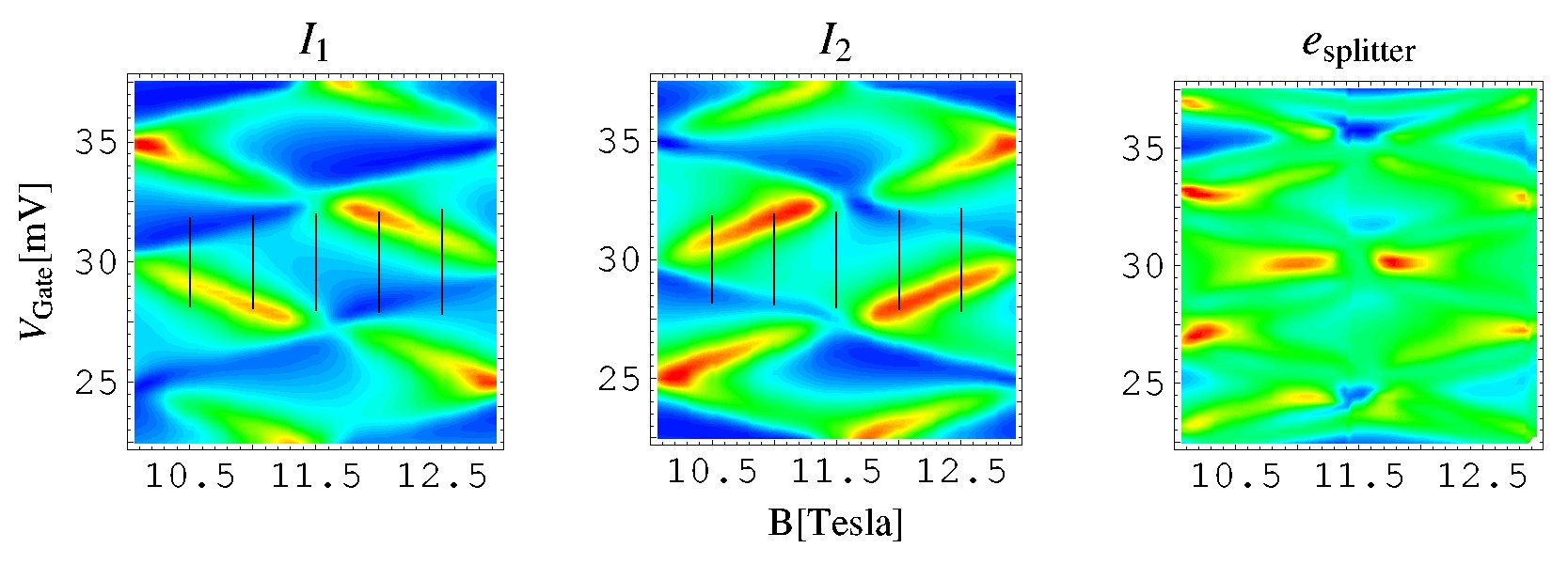
Since in the analytical model of a ring we have already located, as shown in Fig. 4, a good splitter configuration near , the same configuration (with some effective mass) would be a convincing place to look for a splitter using the tight-binding model. We focus on the more realistic low effective mass regime where a bias voltage is needed and on a finite temperature of , which should still leave the system well within the quantum regime. In Fig. 5 we plot the current as a function of the experimentally available parameters - the gate voltage and the magnetic field strength. The familiar asymmetric structure from the previous plots is blurred, but still readily recognizable in the two left panels, while the right panel shows the high effectiveness which can be reached when the magnetic field, the gate voltage and the bias voltage are all appropriately tuned. The location of the effectiveness peak could be easily predicted by the transmission line method previously discussed. Obviously, it would be practically impossible to stumble upon such a fortunate combination of conditions by accident, and any experiment must search for them under the explicit guidance of a model such as the analytical model suggested above.
IV Coulomb Blockade Calculations
IV.1 Charging Energy
So far, we have ignored the energy it takes to inject multiple charges into the small region of the ring. This is of some concern since, as will be discussed below, the charging energy can be very significant here and especially when ring-leads coupling is weak, charging effects can play a major role. To stress this point, consider a device (ring) that is charged with an electron of spin up. The energy it takes to bring another electron with a spin down can be significantly different than in the single electron picture. Can this additional degree of freedom provide means to construct more efficient molecular spin filter and spin splitter devices, or will it prevent their realization?
In general, under our set of assumptions one can expect that when charging effects are neglected, states on the ring will be grouped into pseudo-bands with the same total occupation, having widths of around a few level separations and separated by the order of the Fermi energy (which is usually much greater than the level spacing). The addition of the charging term will shift non-neutral bands up linearly in the charging energy with an increasing slope for charged configurations. One should be able to compensate for these changes by using a gate or bias voltage, as discussed below.
One of the simplest ways of taking the charging energy into consideration in the regime of strong charging energy and weak lead binding is within a multi-electron master equation approach.Beenakker91; Kinaret92; Bonet02; Hettler03; Datta2004; Elste05; Braig05; Mukamel06; Hanggi2006; Nitzan07 The correctness of the method requires that the effects of broadening be negligible, which is quite generally not true, but the approximation nevertheless provides some insight into the behavior of nanometric devices when charging has been accounted for, particularly when a nonzero bias has been applied. This formalism is statistical only, and unfortunately this makes discussion of perfect devices that send every electron to the right place more difficult than it is in the single-electron formalism. Alternatively, one can utilize a perturbation treatment in the lead-device coupling, recently suggested by König and Gefen for an AB mesoscopic ring,Gefen02 however, this approach is limited to off-resonant transport only.
Before we proceed to discuss the calculation of the current within the multi-electron master equation approach, we briefly digress to the matter of estimating the charging energy and its variation with ring geometry. Calculating the energy needed to (uniformly) charge a ring or torus is an elementary electrostatics problem, though not one to which an analytical solution exists to our knowledge. The calculation below provides a qualitative estimate of the magnitude of the charging energies and the numbers should not be taken as being accurate to within more than an order of magnitude.
The details of the calculation are as follows. As a model we used for simplicity a cylinder of radius and height with a cylindrical hole of radius through its axis (see inset of Fig. 6 for a sketch of the model). The potential at and can be obtained following a standard procedure,Jackson and is given by:
| (17) |
The charging energy for a single electron may then be found by setting to inside the ring and zero otherwise:
| (18) |
The charging energy for electrons is then given by where is the neutral number of electrons.
In Fig. 6 we plot the charging energy of a nanometric ring as a function of the cylinder radius and height . For typical rings considered in this work with a radius of , a height of , and the charging energy is of the order of . For smaller dimensions the charging energy increases considerably and can exceed several electron volts for sub-nanometer rings.
IV.2 Calculating the Spin Current
If one neglects spin-dependent multi-electron effects, then it is formally straightforward to construct from the set of one-electron Hamiltonian and spin eigenfunctions an anti-symmetric basis of multi-electron wavefunctions:
| (19) |
Here is the antisymmetrization operator and the states are identified by their (spin-dependent) level occupations ( or for fermions). Using this anti-symmetric multi-electron wavefunction we can uniquely and conveniently determine the matrix elements of a general many-body operator according to the Slater-Condon rules where only single electron integrals are taken into account:
| (20a) | |||
| (20b) | |||
| (20c) | |||
| (20d) | |||
| (20e) | |||
where is the number of single-electron levels taken into account, and . Multi-electron effects will be considered only in the form of charging energy. Since these values will be used in a rate-process calculation rather than a full quantum formulation, constructing the multi-electron states themselves is actually redundant, and Eqs. (20b)-(20e) along with the single particle data will provide all the necessary information.
In order to perform a master equation based estimation of the current, the transfer rates between different multi-electron states must first be calculated.Beenakker91; Kinaret92; Bonet02; Hettler03; Datta2004; Elste05; Braig05; Mukamel06; Hanggi2006; Nitzan07 We will assume that only levels near the Fermi energy will take part in conduction. This implies that the levels closest to the Fermi energy will be used to construct the multi-electron states themselves using Eq. (20b), with the additional charging term .
The transfer rate through lead between two multi-electron states is given by:
| (21) |
We label multi-electronic states by the Greek indices and . Single electronic levels are labeled by the indices and . We also define the total transfer rate summed over all leads:
| (22) |
In the above equations, is related to the the imaginary part of the self-energy in the single electron picture. To lowest order, if the two multi-electronic states differ only by the occupation of level , if they differ only by and and . Otherwise . This follows from the Slater-Condon rules (cf., Eqs. (20c) and (20d). is the matrix element of the imaginary part of the self-energy. in Eq. (21) is related to the Fermi-Dirac function, :
| (23) |
where is the number of electrons in state .

With the rates known, the linear master equation system can be written as the condition for steady-state:
| (24) |
where is the probability that the system is in a multi-electron state . Once the steady-state occupation probabilities have been solved for the current can be expressed asBeenakker91; Kinaret92; Bonet02; Hettler03; Datta2004; Elste05; Braig05; Mukamel06; Hanggi2006; Nitzan07:
| (25) |
where
| (26) |
Intuitively, this expression states that current flows out of lead whenever an electron flows from it into the device, with the inverse also true. Following a similar line of physical reasoning leads to an expression for spin-polarized current: up or down current flows out of lead whenever an up or down electron flows from it into the device. Assuming no coupling between levels with different spin, the spin-dependent current is given by:
| (27) |
and
| (28) |
Here, where for spin up or down, respectively.
Peaks in the differential conduction as a function of the bias voltage can be expected whenever there exists a difference in energy between two states differing in their number of electrons by one, which is occupied in one lead but not the other, i.e., when the conduction window grows to contain a spectral line. This is why levels spaced more than about from the Fermi level should not take part in conduction within this formalism: transfer through them involves electrons or holes (referring here to level vacancies) not present in the leads.
IV.3 Spin Filter
A filtering device remains straightforward in this formalism, and the previous discussion in subsection III.2 pertains to it as well. Several differences are nevertheless evident. In the single electron formalism a device will conduct at zero bias when the chemical potential coincides with an energy level on the device. In the master equation formalism this still happens when the charging energy is zero. Under such conditions, the difference in energy between the neutral state and the first charged state always equals the Fermi energy, and this difference is obviously contained in the zero-bias conduction window.
In the presence of charging, the picture is somewhat more involved. The same states discussed above are now shifted differently by charging since they have a different number of electrons. For the sake of clarity, we will first consider the simplest case where only levels and thus states are included. We assume that the system can have electrons, electrons, or electrons with energies , , and , respectively ( is the single electron level energy). Furthermore, is the neutral occupation and we assume it is such that one of the aforementioned levels is occupied when the systems is neutral. The value of these energies was calculated by taking the single electron level and adding charging terms ( for both and ) and magnetic field splittings (for the state).
When the chemical potential in one of the leads equals the energy difference between multi-electron states a peak will appear in the differential conductance. For the case described here when the bias voltage falls symmetrically on both junctions, conduction peaks will occur when the energy difference between two multi-electron states of different occupations is equal to the value of the lead Fermi energy combined with half the applied bias voltage. Taking the Fermi energy as that of the lower of the two single electron conduction levels, the conduction peaks are expected to appear at and (these peaks are doubly degenerate).
Typical behavior of a spin filter device is illustrated in Fig. 7, where , , and . On the left, surface plots of the current as a function of the gate and bias voltages are shown (panels (a)-(d)). Upper panels show the current of spin up (left) and spin down (right) electrons for a wide range of gate and bias voltages. Note how current steps (or conduction peaks) occur whenever the conduction window cuts across a difference between state energies as discussed above. For instance, with no gating transitions with occur simultaneously at , and with a gate voltage of the first step occurs at zero bias. On the scale of the plots shown in panels (a) and (b), the currents for the two different spins are almost indistinguishable. The difference in current between the two polarization can be seen in panels (c) and (d), where we zoom in on a specific area of the line described by , where is the gate voltage. Here, one spin starts to flow at slightly lower bias voltages, the current rising with the voltage to a high peak and then falling back down as the other spin begins to flow as well. A plane cut through this surface is shown in panel (e), where it is clearly demonstrated how by tuning the voltages a spin filter can still be constructed when charging is taken into account. A symmetric filter for the opposite spin type is found when inverting the gate voltage. As can be seen in the figure, the first conduction peak occurs at and the second occurs at . As a result of the broken symmetry, these peaks are non-degenerate and correspond to transition with . The other two peaks corresponding to will occur at a significantly higher bias voltage. This is in contrast to the simple example where only states were considered, as describe above, where the current peaks are degenerate and appear simultaneously.
One of the interesting features shown in Fig. 7 is the negative differential spin conductance of the spin up electron (panel (g)). This is explained by the sudden drop in the population of the state (corresponding to a conduction electron of spin up) as the change in chemical potentials begins to allow the population of state (corresponding to a conduction electron of spin down). This population switching is reminiscent of the nonmonotonic change of occupation in two electrostatically coupled single-level quantum dots.Gefen05; Oreg05 The state populations are shown in panel (h) of Fig. 7. The drop in the spin up state population is correlated with the occurrence of negative differential spin conductance (the conduction is normalized to the maximal value Beenakker91). This can be explained in the following way: the current for each spin is determined by the product of the probability that the system is in state and the rate of transitions between state and state (which is the state with no conducting electrons), where is for spin up conducting electron and for spin down conducting electron. We therefore expect that at chemical potentials where the relevant Fermi functions and hence the rates are nearly constant, the current will be approximately proportional to the population.
IV.4 Spin Splitter
The discussion of the spin splitter within the multi-electron master equation is more involved than the spin filter and requires at least levels ( states). We assume that at (the neutral occupation) two of the four conduction levels are occupied. Having previously established a way in which single electron levels suitable for spin splitting can be found on a ring, we focus on the effects of charging. First, and for the moment neglecting charging energies, we assume that we have found two levels with energies that are spin degenerate without Zeeman splitting, with the following properties: they should be adjacent (other than perhaps for non-transmissive levels, which will not qualitatively affect our results), and should both be coupled symmetrically to the input lead, while each is coupled to a single different output lead. Other levels should be at least away in energy. All couplings are taken to be the same and diagonal couplings are ignored. Accounting for Zeeman splitting will simply shift each of these levels in energy by without modifying the coupling. As before for the single electron picture, the coupling between levels with different spins is neglected. An example of such a case is discussed above in Sec. III.3 where is given in terms of the ring level spacing (c.f., Eq. 15 and Fig. 4).
Setting the chemical potential of the input lead to and both output chemical potentials to , it should now be clear under both formalisms that without charging energy a perfect spin splitter exists at , as shown in the upper panels of Fig. 8. In the single electron picture this happens as two levels with opposite spins and different lead bindings enter the conduction window. In the multi-electron master equation this happens when the difference in energy between states and states enters the conduction window. These two conditions are equivalent for .
Including charging effects will cause the states to move up in energy by . This has the effect of repositioning the conductance peaks at . If is of the order of the Zeeman term then the charging energy will interfere with the structure that allowed our spin splitter for , since the energy difference between states that differ by one electron of both spin up and spin down can become similar. On the other hand, if the charging energy is increased further, the transitions and become distinguishable in energy. One way to take advantage of this is to apply a gate potential in order to shift the state energies by so that only the transitions are in the conduction window (new transitions may appear at similar energies if other levels are too close, but since level spacing for a ring generally increases with energy we can neglect such contributions). Once again at perfect splitting occurs, though at a smaller total current, since fewer state transitions are involved. This is apparent in the lower panels of Fig. 8.
V Conclusions and Directions for Further Study
We have investigated several ways in which rings or ring-like structures with a radius of the order of nanometers, coupled to metallic leads, might be used to construct simple spin-sensitive devices. We have focused only on the Zeeman splitting to differentiate between spins, since it is always present while other effects commonly utilized in microscopic structures, such as the Rashba and Dresselhaus effects, are generally absent in molecular/nanometric structures. We believe the niche this work occupies in the search for nanospintronic devices is yet unexplored: very small coherent structures and weak spin-dependent effects have not received much attention, despite their formal simplicity and significance. What we have shown here is that although building devices under the burden of such limitations is difficult, it is possible. Considering the scientific and technological benefits of such devices we believe it will also be worthwhile.
The basic calculations we have performed are enough to point one in the right direction as to the desired properties of molecule-sized Aharonov-Bohm spin devices and the conditions which their desired operation might be observed. A similar methodology can be applied to more complex devices or sets of devices. The actual devices specifically discussed here were two of the most basic - a spin-filter and a spin-splitter or Stern-Gerlach device. However, the conclusions drawn and principles laid out may easily be extended to many interesting systems, from quantum gates (since in theory we can use interference devices to perform general unitary transformations between input and output gates) to molecular memory (since an electron trapped on the device will modify its electrical properties and thus may be detectable at a later time).
Several complementary methods were utilized during the course of this investigation: first, a simple single-electron, analytical model in which the parameter space can easily be explored, and thus basic intuition about the system can be gained. Second, a tight-binding nonequilibrium Green’s function treatment, which incorporates a more realistic physical structure that can be compared directly with experimental data, but still assume independent electrons, was applied to similar systems studied within the simple analytical model. Finally, a multi-electron master equation approach that can be used to examine many-particle effects was grafted onto the tight-binding results. Here, we choose to focus on electric charging, since its effects are energetically dominant.
Our analysis of the filter, meant to be a test-case, was based on the study of the spinless case where it was possible to create very narrow conduction peaks near zero magnetic field by combining weak device/leads couplings and a gate voltage to shift the conduction resonances to .Hod2004; Hod2005a; Hod2005b; Hod2006a Since the Zeeman splitting depends linearly on the magnetic field, a spin filter always requires a finite magnetic field, at least high enough to separate the spin conduction peaks in energy by more than . Control over the position of the spin-dependent conduction peaks and their widths can be achieved by carefully adjusting the kinetic phase and the coupling between the device and the leads, respectively. Unlike the spinless case where , the kinetic phase is now a function of the magnetic flux itself, and thus, the conduction is not a simple periodic function of the parameters. High efficiency spin filters are constructed at the highest magnetic field possible, where spin-dependent effects are strongest, and flexibility is gained by selecting materials or structures with high effective mass (or large ring size, which is not desirable). Charging effects do not drastically modify this picture since spin selectivity depends only the Zeeman term and the application of a gate voltage can compensate for the charging energy itself. However, charging leads to a breaking of symmetries and as a result to negative differential spin-conduction.
The physics of the spin splitter device is similar to that described above with the added complication that differentiated control of the spin-dependent wavefunction at the different leads is required. Within the single electron picture, a spin splitter device may operate when two spin-degenerate levels exist such that one transmits through one lead only and the other through the other lead only. Furthermore, the level separation should equal exactly the Zeeman splitting. Alternatively, the level separation can be compensated for by the application of a bias voltage, as long as there are no transmissive levels between the two spin-degenerate levels. Here, parameter space includes the ring size, effective mass, device-leads couplings, and the angles between the output leads. Increasing the effective mass, as before, reduces the level spacing on the ring, thereby enabling the construction of spin splitters at lower magnetic fields and with smaller dimensions. Charging breaks the symmetry and can reduce the overall current through the device. However, charging does not abolish the general picture and the application of a gate potential can be used to overcome most of its effects.
For both prototype devices we have shown how the limits of lead-coupling, system geometry and temperature at which one might expect to see the desired effects can easily be estimated, as well as several ways in which one can implement specific behaviors by systematically finding parameters at which they occur, either exactly or approximately. We have also shown that even within the parameters space of a device formed by a single ring with two or three leads, nontrivial behaviors with useful properties take place. In at least two instances, we have made a case that our findings are physical rather than a mathematical peculiarity of some model by reproducing them under different assumptions and formalisms. We have found an interesting example of negative differential conductance for a spin polarized current with a simple explanation. Finally, we have described what is, to our knowledge, the smallest Stern-Gerlach apparatus ever reasonably conceived of, and one which is fully switchable in directionality at constant magnetic field by the application of an external electric field.
Despite their simplicity, the calculations reported here provide several novel predictions that seem to be model independent. Nevertheless, more refined models are an important set of directions to continue along. In particular, drawing from the study of crystals and mesoscopic systems, we see ways of enhancing the effect of Zeeman splitting which require a more elaborate electronic structure description. One such is through the effects of spin-orbit coupling and the local spin density exchange-correlation energy, both of which have been used to explain the giant spin -factor enhancement that has been observed in mesoscopic structures under certain conditions.Majumdar98 It is quite possible that the same effect can be recreated with discrete levels, although this probably requires that only a small number of levels be occupied (corresponding once again to very low electron densities).
While we have studied only two- and three-terminal devices, with only one injective terminal, it is reasonable that four terminal devices will also be of interest as coherent quantum gates. One of the reasons we have found it worthwhile to draw attention to the importance of many-particle effects is our hope that in time-dependent calculations they may be used to create sequential logical behavior without sacrificing coherence - for instance, an electron may only be able to enter the device through one lead, but when it enters it opens up another lead, and the inflow of another electron causes both to be discharged through a third lead - a sort of sequential AND gate, two of which could form a true AND gate. Of course, to consider useful computation it is necessary to model entire networks of such gates, where input electrons enter on one set of leads, propagate throughout the network and leave it on another set of leads. Such a network presents new delocalized challenges unless devices are somehow coupled in such a way that no inter-device interference takes place. However, even if the devices within the network are all ”imperfect” devices that only approximate logic gates, as long as every device has independently adjustable parameters (like a gate voltage) such a network forms a fascinating basis for a model of a quantum neural networks. These and related issues are still open for future study.
VI Acknowledgments
We would like to thank Roi Baer, Yuval Gefen, Andrew Millis, Yuval Oreg, Yoram Selzer, and Amir Yacoby for discussions and suggestions. This work was supported by the EU under the program SA-NANO (grant number STRP 013698).
References
- (1) Y. Aharonov and D. Bohm, Phys. Rev. 115, 485 (1959).
- (2) R. A. Webb, S. Washburn, C. P. Umbach, and R. B. Laibowitz, Phys. Rev. Lett. 54, (1985).
- (3) G. Timp et al., Phys. Rev. Lett. 58, 2814 (1987).
- (4) A. Yacoby, M. Heiblum, D. Mahalu, and H. Shtrikman, Phys. Rev. Lett. 74, 4047 (1995).
- (5) A. van Oudenaarden, M. H. Devoret, Y. V. Nazarov, and J. E. Mooij, Nature 391, 768 (1998).
- (6) A. Fuhrer et al., Nature 413, 822 (2001).
- (7) S. Zaric et al., Science 304, 1129 (2004).
- (8) R. Leturcq et al., Phys. Rev. Lett. 95, 126603 (2005).
- (9) J. Nitta, F. E. Meijer, and H. Takayanagi, Appl. Phys. Lett. 75, 695 (1999).
- (10) D. Frustaglia, M. Hentschel, and K. Richter, Phys. Rev. Lett. 87, 256602 (2001).
- (11) I. Malajovich, J. J. Berry, N. Samarth, and D. D. Awschalom, Nature 411, 770 (2001).
- (12) E. I. Rashba, Sov. Phys. solid. State 2, 1109 (1960).
- (13) G. Dresselhaus, Phys. Rev. 100, 580 (1955).
- (14) M. Hentschel, H. Schomerus, D. Frustaglia, and K. Richter, Phys. Rev. B 69, 155326 (2004).
- (15) D. Frustaglia, M. Hentschel, and K. Richter, Phys. Rev. B 69, 155327 (2004).
- (16) F. E. Meijer, A. F. Morpurgo, and T. M. Klapwijk, Phys. Rev. B 66, 033107 (2002).
- (17) R. Ionicioiu and I. D’Amico, Phys. Rev. B 67, 041307 (2003).
- (18) D. Frustaglia and K. Richter, Phys. Rev. B 69, 235310 (2004).
- (19) B. Molnar, F. M. Peeters, and P. Vasilopoulos, Phys. Rev. B 69, 155335 (2004).
- (20) U. Aeberhard, K. Wakabayashi, and M. Sigrist, Phys. Rev. B 72, 075328 (2005).
- (21) X. F. Wang and P. Vasilopoulos, Phys. Rev. B 72, 165336 (2005).
- (22) P. Földi, O. Kálmán, M. G. Benedict, and F. M. Peeters, Phys. Rev. B 73, 155325 (2006).
- (23) V. M. Ramaglia, V. C. nad G. De Filippis, and C. A. Perroni, Phys. Rev. B 73, 155328 (2006).
- (24) O. Hod, R. Baer, and E. Rabani, J. Phys. Chem. B 108, 14807 (2004).
- (25) O. Hod, E. Rabani, and R. Baer, J. Chem. Phys. 123, 051103 (2005).
- (26) O. Hod, R. Baer, and E. Rabani, J. Am. Chem. Soc. 127, 1648 (2005).
- (27) O. Hod, E. Rabani, and R. Baer, Acc. Chem. Res. 39, 109 (2006).
- (28) O. Hod, R. Baer, and E. Rabani, Phys. Rev. Lett. 97, 266803 (2006).
- (29) Y. Meir, O. Y. Gefen, and Entin-Wohlman, Phys. Rev. Lett. 63, 798 (1989).
- (30) O. Entinwohlman, Y. Gefen, Y. Meir, and Y. Oreg, Phys. Rev. B 45, 11890 (1992).
- (31) M. Popp, D. Frustaglia, and K. Richter, Nanotechnology 14, 347 (2003).
- (32) Y. Elhassid, Rev. Mod. Phys. 72, 895 (2000).
- (33) C. W. J. Beenakker, Phys. Rev. B 44, 1646 (1991).
- (34) J. M. Kinaret et al., Phys. Rev. B 46, 4681 (1992).
- (35) E. Bonet, M. M. Deshmukh, and D. C. Ralph, Phys. Rev. B 65, 045317 (2002).
- (36) M. H. Hettler, W. Wenzel, M. R. Wegewijs, and H. Schoeller, Phys. Rev. Lett. 90, 076805 (2003).
- (37) S. Datta, Nanotechnology 15, S433 (2004).
- (38) F. Elste and C. Timm, Phys. Rev. B 71, 155403 (2005).
- (39) S. Braig and P. W. Brouwer, Phys. Rev. B 71, 195324 (2005).
- (40) U. Harbola, M. Esposito, and S. Mukamel, Phys. Rev. B 74, 235309 (2006).
- (41) F. J. Kaiser, M. Strass, S. Kohler, and P. Hänggi, Chem. Phys. 322, 193 (2006).
- (42) M. Galperin, M. A. Ratner, and A. Nitzan, J. Phys. Cond. Matt. 19, 103201 (2007).
- (43) H. A. Staab and F. Diederich, Angew. Chem. Int. Ed. Engl. 17, 372 (1978).
- (44) B. Hajgató and K. Ohno, Chem. Phys. Lett. 385, 512 (2004).
- (45) G. P. Collins, Physics Today 46, 17 (1993).
- (46) H. C. Manoharan, C. P. Lutz, and D. M. Eigler, Nature 403, 512 (2000).
- (47) G. V. Nazin, X. H. Qiu, and W. Ho, Science 302, 77 (2003).
- (48) A. G. Aronov and Y. V. Sharvin, Rev. Mod. Phys. 59, 755 (1987).
- (49) D. Frustaglia and K. Richter, Found. Phys. 31, 399 (2001).
- (50) Y. Gefen, Y. Imry, and N. Y. Azbel, Phys. Rev. Lett. 52, 129 (1984).
- (51) R. Landauer, IBM J. Res. Dev. 1, 223 (1957).
- (52) R. Baer and D. Neuhauser, Chem. Phys. Lett. 374, 459 (2003).
- (53) M. P. L. Sancho, J. M. L. Sancho, and J. Rubio, J. Phys. F:Met. Phys. 14, 1205 (1984).
- (54) M. P. L. Sancho, J. M. L. Sancho, and J. Rubio, J. Phys. F:Met. Phys. 15, 851 (1985).
- (55) M. B. Nardelli, Phys. Rev. B 60, 7828 (1999).
- (56) N. W. Ashcroft and N. D. Mermin, Solid State Physics (Brooks Cole, ADDRESS, 1976).
- (57) A. Majumdar, J. Appl. Phys. 83, 297 (1998).
- (58) J. Konig and Y. Gefen, Phys. Rev. B 65, 045316 (2002).
- (59) J. D. Jackson, Classical Electrodynamics (Academic Press, New York, 1998).
- (60) J. Konig and Y. Gefen, Phys. Rev. B 71, 201308 (2005).
- (61) M. Sindel, A. Silva, Y. Oreg, and J. von Delft, Phys. Rev. B 72, 125316 (2005).