ATLAS silicon module assembly and qualification tests at IFIC Valencia
Abstract
ATLAS experiment, designed to probe the interactions of particles emerging out of proton proton collisions at energies of up to 14 TeV, will assume operation at the Large Hadron Collider (LHC) at CERN in 2007. This paper discusses the assembly and the quality control tests of forward detector modules for the ATLAS silicon microstrip detector assembled at the Instituto de Física Corpuscular (IFIC) in Valencia. The construction and testing procedures are outlined and the laboratory equipment is briefly described. Emphasis is given on the module quality achieved in terms of mechanical and electrical stability.
keywords
Solid state detectors, large detector systems for particle and astroparticle physics, particle tracking detectors1 Introduction
The ATLAS detector [1], one of the two general-purpose experiments of the Large Hadron Collider (LHC), has entered into the final stages of installation at CERN. The LHC, a proton-proton collider with a 14-TeV centre-of-mass energy and a design luminosity of , is expected to deliver the first proton beam by the end of 2007. The ATLAS central tracker (Inner Detector, ID) [2] combines the silicon detector technology (pixels [3] and micro-strips [4]) in the innermost part with a straw drift detector with transition radiation detection capabilities (Transition Radiation Tracker, TRT) [5] in the outside, operating in a 2-T superconducting solenoid.

The microstrip detector (Semiconductor Tracker, SCT) [4], as shown in Fig. 1, forms the middle layer of the ID between the Pixel detector [3] and the TRT [5]. The SCT system comprises a barrel made of four nested cylinders and two end-caps of nine disks each. The barrel layers carry 2112 detector units (modules) altogether, while a total of 1976 end-cap modules are mounted on the disks. The whole SCT occupies a cylinder of 5.6 m in length and 56 cm in radius with the innermost layer at a radius of 27 cm.
The silicon modules [6, 7] consist of one or two pairs of single-sided p-in-n microstrip sensors [8] glued back-to-back at a 40-mrad stereo angle to provide two-dimensional track reconstruction. The - thick sensors have 768 AC-coupled strips with an pitch for the barrel and a pitch for the end-cap modules. Between the sensor pairs there is a highly thermally conductive baseboard. Barrel modules follow one common design, while for the forward ones four different types exist according to their position in the detector.
The SCT construction involved —among other development projects and macro-assembly— the building and Quality Control (QC) of modules. In particular, the assembly of the required 1976 ATLAS SCT forward modules [7] plus a contingency of 20% was distributed among 13 European and one Australian institutes, divided into three clusters in order to facilitate the sharing of tasks and the flow of components. The IFIC group, as a member of the UK-V cluster, followed the complete assembly sequence and all the necessary QC tests were performed, as shown in Fig. 2, for all assembled modules. The full production was launched after a qualification period, during which the tooling and the execution of the procedures were successfully validated.

The IFIC-SCT group assembled and tested a total of 282 forward SCT modules; 125 outer modules and 157 long middle ones. Before the production startup, the Valencia group initially undertook the construction of 125 outer and 96 middle modules. After a re-organisation of the forward modules production, the group accepted the responsibility to assemble a surplus of 61 middle modules, which amounts to a 28% increase with respect to the initial commitment.
This paper begins with a brief description of the module assembly and QC sequence in Sec. 2, followed by a report on the metrology procedure and respective measurements in Sec. 3. In Sec. 4, the front-end electronics and the electrical setup and tests are outlined, and the corresponding results are reported. Some studies performed on modules assembled in other sites are discussed in Sec. 5. An overview of the QC tests results and the conclusions are given in Secs. 6 and 7, respectively.
2 Module assembly and quality control overview
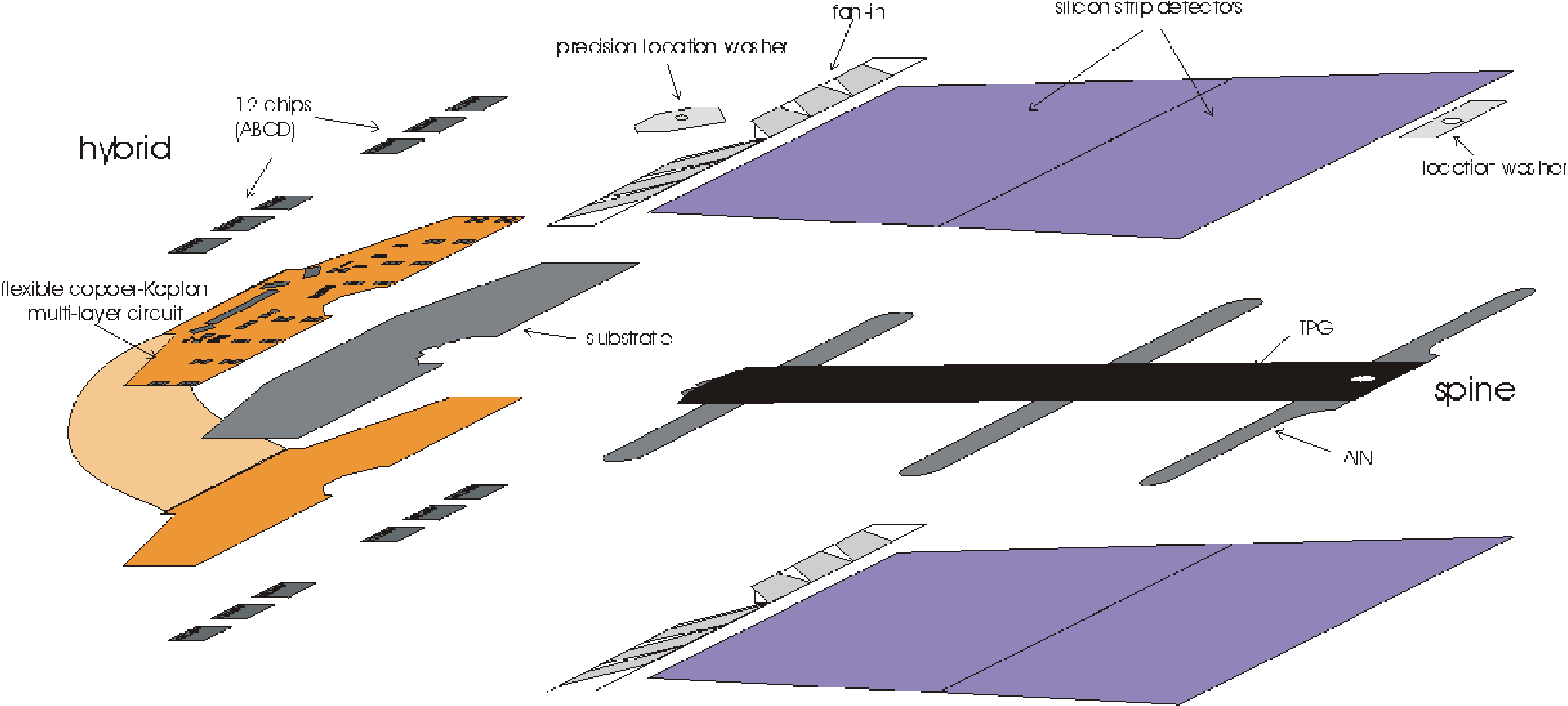
The forward silicon modules [7] consist of one or two pairs of single-sided p-in-n micro-strip sensors glued back-to-back at a 40-mrad stereo angle, as shown in Fig. 3, to provide two-dimensional track reconstruction. The 285- thick sensors [8, 9] have 768 AC-coupled strips implanted with a pitch of . Between the sensor pairs there is a highly thermally conductive baseboard (spine) [9]. The sensors are connected to the front-end electronics board (hybrid) [10] by means of fan-ins11 1 Parts made of glass with aluminum traces, providing electrical connection channel-by-channel from the sensors to the read-out chips and mechanical connection between the hybrid and the detector part of the module. [9]. Barrel modules [6] follow one common design, while for the forward ones four different types exist based on their position in the detector. At IFIC, outer and long-middle modules were built made up out of two pairs of Hamamatsu22 2 Hamamatsu Photonics Co. Ltd., 1126-1 Ichino-cho, Hamamatsu, Shizuoka 431-3196, Japan. silicon sensors.
In order to carry out the module production according to the quality criteria set by the ATLAS SCT collaboration, dedicated machinery and tooling was constructed and installed in a clean room of at IFIC, where temperature was controlled within and relative humidity within 5% (keeping it below 50%). This area was divided into two compartments: a small one () of class 1000 and a big room () of class 10 000. In the former the electrical properties of the sensors and modules were measured and the visual inspection of the components was performed, while in the latter the remaining assembly and testing tasks took place.
Besides the production-oriented infrastructure, a laser test bench has been developed aiming at various studies on silicon detectors —including SCT modules. Specifically, measurements were carried out in order to detect defects on strips [11]. Important characteristics of module performance were determined with the laser beam, such as the response dependence on interstrip position, the pulse shape reconstruction for different impact positions along the strip, the spatial resolution, etc.
The end-cap module comprises several components [9], viz. the silicon sensors, the spine, the fan-ins, the washers and the electronics hybrid [10], assembled as shown in Fig. 3. Tests were made upon reception and during assembly to assure that the components have not been damaged during transport or in the first stages of module construction, including a first scan of the individual silicon sensors. In the following, the module assembly steps and intermediate quality checks, described in full detail in Refs. [7, 12, 13, 14], are outlined and only the technical features specific to the IFIC laboratory are mentioned.
- Sensor pair alignment.
-
To achieve good tracking performance stringent requirements on the positioning of the modules are imposed. The precise alignment [13] of the detectors is achieved by employing a robot consisting of six linear stages,33 3 Nappless-Coombe Ltd. pictured in Fig. 4a. It is equipped with an optical system for pattern recognition and stages which are commanded by the DMC-1500 controller44 4 Galil Motion Control, Inc. through a PC using a program running under LabVIEW developed at the University of Manchester [15]. The detectors and the fan-ins are kept in place through vacuum chucks on the assembly station and their positioning is achieved through four fiducial marks on the turn plate, shown at the centre of Fig. 4b. After the alignment, the detectors, the fan-ins and the hybrid are mounted on the turn plate, by means of the transfer plates (Fig. 4b, top left and right), and they are then transferred to the glue dispenser (Fig. 4c).

(a) Alignment and assembly stand. 
(b) Assembly tooling. 
(c) Dispenser machine. Figure 4: Alignment, assembly and gluing apparatuses for module building. - Glue dispensing.
-
The glue dispensing device, shown in Fig. 4c, works on a Sony Cast Pro system with a dispensing system attached and controlled by a PC using the LUNA language. The thermally conductive glue applied is a two-component, room-temperature curing epoxy55 5 Araldite 2011, supplied by Ciba-Geigy. [9]. The mixture makes an adhesive of adequate strength and high thermal conductivity.
- Detector assembly and glue curing.
-
After applying the glue, each transfer plate consecutively is inserted in and fastened to the turn plate at the same place where it was when the aligned detectors were picked up from the assembly station. The module components are then left to cure in a four-pillar stand for several hours.
- Detector scan and alignment check.
-
The measurement of the electrical properties of sensors and the visual inspection of the components [14] takes place in a probe station comprising a microscope and a position controller installed in a dark box, as shown in Fig. 5a. The electrical properties of the silicon sensors were examined using the home-designed program Probe [16]. It is a C++ program using the graphical user interface package Qt, running under Linux, which controls the measurement instruments66 6 Keithley 237 HV source measure unit; Keithley 236 source measure unit; Wayne Kerr 6425 Precision Component Analyzer; Pickering switching matrix; and Keithley 2700 multimeter. via an IEEE488 interface.
- Hybrid assembly with fan-ins and washers.
-
The hybrid [10] is lowered onto its correct position on the turn plate by inserting small tapered pins through the hybrid holes. Conductive glue is applied underneath the HV tongues to ensure connection to the detector back-planes. These electrical connections and the absence of short circuits is checked before going to the next step. The fan-ins [9] are added later using the fan-ins chucks, shown in Fig. 4b (bottom), and the glue dispensing machine. The fan-ins chucks are positioned using location pins of the proper side of the turn plate and they are tightened with screws. The procedure is completed with the fitting of the location washers [9] on the module.
- and survey.
- Wire-bonding.
-
All the production modules are wire-bonded by the fully automatic bonder machine77 7 K&S 8090. pictured in Fig. 5b. The laboratory is also equipped with a semi-automatic bonder88 8 K&S 1470. used during the pre-qualification period. A pull-tester,99 9 Dage 3000 shown in Fig. 5c, was also used during the qualification period for the validation of the bonding parameters.

(a) Probe station. 
(b) Automatic bonding device. 
(c) Pull-testing machine. Figure 5: Devices for module testing and wire-bonding. - Thermal cycling.
-
When the assembly is completed, the modules undergo a thermal cycling in order to verify that temperature variations do not compromise the geometrical properties of the module [18]. This task is performed in a climate chamber,1010 10 Dycometal CM 40/125A. displayed in Fig. 6a, which operates at a temperature ranging from to . An aluminium rack positioned inside the chamber, shown in Fig. 6b, allows simultaneous thermal cycling of up to six modules. The thermistors are readout by a multimeter1111 11 Keithley 2700. and the system is controlled, monitored and read out by a PC. The thermistors temperature was recorded every 10 s in a data file and plotted on-line (cf. Fig. 6c). During this process the thermistors temperature varies from to for a total of ten cycles lasting about 3.5 h each.

(a) Thermocycling setup. 
(b) Interior of climate chamber. 
(c) Thermal cycle. Figure 6: The thermal cycling setup and a typical monitoring plot. The oven and thermistor temperatures are plotted, together with the relative humidity. A complete process covers ten cycles.
The quality assurance plan for the forward modules foresees the following QC tests [14] for the completed (glued and bonded) module:
3 Metrology
The precision needed during construction is determined by physics requirements. For the detector to be hermetic in tracks with , a tolerance of in the direction and in radius is specified [18]. Taking this into consideration, the effective module dimensions specifications are derived [17].
3.1 Setup and procedures
The metrology process is divided into two main tasks (see Ref. [17] for a detailed description); the metrology,1212 12 The -axis is defined along the strips and the -axis is perpendicular to them and on the sensor plane. in which relative in-plane alignment between silicon sensors and the mounting hole and slot1313 13 As hole is denoted the mounting point between the hybrid and the sensors, whereas the slot is located in the module endpoint. are measured, and the -profile of the detectors relative to the mounting surface. The position of sensors in the -plane is defined by a number of fiducial marks printed on its surface. The hole and mounting slot have a sharp and well-defined edge which is used for determining its position.
The metrology parameters, which refer to the relative positions of the four detectors in the -plane with respect to each other, are the following:
- •
, , which represent the front-to-back detector pair alignment in and ;
- •
and , which represent the separation between the detectors of each side;
- •
angle, which denotes the deviation from the nominal stereo angle () between the two detector pairs;
- •
, , , and , which are the four individual detector angles relative to their nominal position; and
- •
, , , , are the hole and slot positions in and , respectively.
The specified nominal values and the corresponding tolerances for these parameters are listed in Table 1.
| Parameter [unit] | Nominal value (middle) | Nominal value (outer) | Tolerance |
| [mm] | 71.708 | -78.136 | 0.020 |
| [mm] | 0.000 | 0.000 | 0.020 |
| [mm] | -66.672 | 62.244 | 0.100 |
| [mm] | 0.000 | 0.000 | 0.020 |
| [mm] | 0.000 | 0.000 | 0.010 |
| [mm] | 0.053 | -0.040 | 0.005 |
| , [mm] | 59.900 | 61.668 | 0.010 |
| – [mrad] | 0.000 | 0.000 | 0.130 |
| [mrad] | -20.000 | -20.000 | 0.130 |
The metrology,1414 14 The -axis is defined vertical to the module. on the other hand, is performed by measuring the position of a grid of 25 points distributed over the surface of each of the four detectors, as shown in Fig. 7. From these points, the average (), the maximum (), the minimum () and the RMS () values are calculated for the front and back side of the module. These parameters are then compared with the specifications, which are listed in Table 2 [17].

| Module side | Nominal value (mm) | Tolerance (mm) |
|---|---|---|
| Front | 0.875 | 0.115 |
| Back | -0.375 | 0.115 |
A custom-made1515 15 AIDO-IFIC. laser interferometry metrology system, shown in Fig. 8 was employed for the mechanical survey of the module, providing an accuracy of . It is equipped with two cameras to achieve a better accuracy in the determination of the parameters. Thus it avoids errors due to intermediate manipulation steps when turning the module upside down, as is needed with single camera systems. During the survey, the module is mounted in a frame allowing the measurement of the and positions of the detectors of both sides with respect to the same reference points.

3.2 Measurements
As mentioned before, the module dimensions were measured twice: just after gluing the components together and before wire-bonding, and once more after the thermal cycling. The overall final-measurement results for all 13 parameters are shown in Fig. 9. The majority of the modules are well within the specifications, apart from some cases where parameter exceeds the allowed limits. These cases stand for the majority of the modules characterised as Pass.


The thermal cycling did not affect the metrology parameters, whereas, in some cases, it altered the profile. Parameters , and for both sides —in particular — decreased after the thermal treatment in several modules, namely they appeared slightly bent in the centre. However, this effect, did not have any impact whatsoever on the production yield. The distributions of the parameters are presented in Fig. 10.


4 Electrical performance
The readout of the SCT modules is based on 12 ABCD3TA [20] ASICs mounted on a copper/kapton hybrid [10]. The ABCD3TA chip features a 128-channel analog front end consisting of amplifiers and comparators and a digital readout circuit operating at a frequency of 40.08 MHz. It utilises the binary scheme, where the signals from the silicon detector are amplified, compared to a threshold and only the result of the comparison enters the input register and a 132-cell deep pipeline, awaiting a level-1 trigger accept signal. It implements a redundancy mechanism that redirects the output and the control signals, so that a failing chip can be bypassed. To reduce the channel-to-channel threshold variation, in particular after irradiation, the ABCD3TA features an individual threshold correction in each channel with a 4-bit digital-to-analog converter (TrimDAC) with four selectable ranges. The clock and command signals as well as the data in binary form are normally transferred from and to the off-detector electronics through optical links [21], however during the production electrical tests, the ASICs were read out electrically using a pseudo-optical scheme. Two streams of data are read out, one for each module side (768 channels).
In this section the electrical specifications and the respective quality control procedures are outlined. Among the various functionality tests of the readout part of the module, only the more crucial ones such as the gain and the noise measurements are elaborated. Some exceptional cases are also discussed in detail. A complete description of the electronics test procedure is available in Ref. [19].
4.1 Specifications and setup
The LHC operating conditions demand challenging electrical performance specifications for the SCT modules and the limitations mainly concern the accepted noise occupancy level, the tracking efficiency, the timing and the power consumption. The Equivalent Noise Charge (ENC) is specified [22] to be less than 1500 electrons before irradiation. The noise hit rate is required to be per strip at the ATLAS SCT operating threshold of 1 fC. At this threshold an efficiency of 99.5% is expected before irradiation, however a threshold higher than 1 fC might be needed after irradiation to meet the efficiency and noise occupancy specifications [7]. As far as the tracking performance is concerned, a starting requirement is a low number of dead readout channels, specified to be less than 16 for each module to assure at least 99% of working channels. Furthermore no more than eight consecutive faulty channels are accepted in a module.
A standard DAQ system has been developed within the ATLAS SCT collaboration aiming at verifying the hybrid and detector functionality after the module assembly and at demonstrating the module performance with respect to the required electrical specifications. During the electrical tests the modules are mounted in a light-tight aluminum box which supports the modules at the two washers. The test box includes a cooling channel connected to a liquid coolant system.1616 16 Huber chiller with antifreeze as a coolant. The operating temperature is monitored by a thermistor mounted on the hybrid. The box also provides a connector for dry air circulation. Subsequently, the module test box is placed inside the custom-made, light-proof box, shown in Fig. 11 (left), and it is electrically connected to the readout system and VME crate. Up to six modules can be tested simultaneously with this configuration. The grounding and shielding scheme of the setup is of crucial importance, therefore a careful optimisation is necessary.


In all the measurements performed, the ASICs are powered with three standard SCT low-voltage power supplies, SCTLV, and read out electrically via a system, comprising one SLOG, one MUSTARD and one AERO board, installed in two VME crates as pictured in Fig. 11 (right). Two SCTHV high voltage units provided detector bias to the modules. A second complete setup including the respective readout system was also built, to serve as a backup in the event of failure of the first one. A detailed description of the SCT readout system is given in Refs. [19, 7].
4.2 Testing sequence
To determine the front-end parameters of the modules, an internal calibration circuit that simulates an input charge in the range is implemented in the ASICs. By injecting various known charges and performing threshold scans, the analogue properties of each channel can be determined, such as the gain, the offset and the noise. A complementary error function is fitted to each threshold scan to determine the point of 50% efficiency () and the output noise for each channel. A multi-parameter fit to a set of points is used to obtain the response curve from which gain and offset for each channel are derived. The input noise is thus calculated by dividing the output noise measured at over the calculated gain. The testing sequence followed in Valencia is the following:
- Long-term test:
-
This is a burn-in test, during which the ASICs are powered, clocked and triggered for 24 hours while the module bias voltage is kept at 150 V and its thermistor temperature is . The bias voltage, chip currents, hybrid temperature, the leakage current and the noise occupancy are recorded every 15 min. Moreover, every two hours a so-called confirmation1717 17 It includes digital tests, a strobe delay setting and a three-point gain. test is performed to verify the correct functionality of the module.
- Characterisation:
-
A full electrical characterisation of the module is carried out at a hybrid operating temperature of and a bias voltage of 150 V, consisting of the following tasks:
- a)
Digital tests: checks of the redundancy links, the chip by-pass functionality and the 128-cell pipeline circuit, executed in order to identify chip or hybrid damage.
- b)
Strobe delay: an optimisation of the delay between the calibration signal and the clock on a chip-to-chip basis.
- c)
Three-point gain: a first evaluation of the gain for three different values of injection charge.
- d)
Trimming: adjustment of the TrimDAC for each channel to allow for an improved matching of the comparators thresholds.
- e)
Response Curve: final measurement of the gain for ten values of injected charge ranging from to .
- f)
Noise occupancy: a threshold scan without any charge injection, performed to yield a direct measurement of the noise occupancy at the equivalent input charge of 1 fC, which is the operating threshold for the SCT module. The adjusted discriminator offset is applied to ensure a uniform measurement across the channels.
- g)
Time walk: a strobe-delay scan is performed to assess the sensitivity of the pulse timing to the injected charge.
- a)
- Final scan:
-
A final measurement of the detector leakage current as a function of the bias voltage ( curve) is performed at to assure that the current drawn by the whole module is low enough for the safe operation of the detector. The current values at 150 V and 350 V are recorded and compared with those of previous curve measurements before and after the module sub-assembly.
The characterisation sequence is also applied as a reception test of the unassembled hybrids.
4.3 Electrical results
Collective results, as far as noise is concerned, are presented in Figs. 13 and 13, for middle and outer modules separately. Middle modules, being shorter than the outer ones,1818 18 In middle modules the total strip length is 117.7 mm, whereas in outer modules it is 121.2 mm. exhibit a lower noise level. The noise occupancy distributions lie well below the specification of . It is worth noting that the acquired noise measurements largely depend on the specific setup optimisation level (e.g. grounding, shielding), therefore these values represent rather an upper limit on the actual module noise. The noise also depends on the hybrid temperature increasing by per degree Celsius. Since under standard conditions at the LHC the modules will operate with a thermistor temperature near —whilst the reported measurements took place at —, a lower noise level than the one obtained during quality control tests is expected during running. Furthermore, the implementation of the grounding, shielding and power distribution scheme guarantee the stability and low-noise operation of the modules when assembled into large structures (disks, cylinders), as demonstrated in subsequent noise measurements [26].


The distributions of the number of defective channels per unassembled hybrid and per module are shown in Fig. 15. These include types of critical defects, such as dead, stuck, noisy channels, channels that have not been wire-bonded to the strips and channels that cannot be trimmed (untrimmable). These channels are masked during normal operation and are practically lost. Also included in the distributions are less critical faults such as low or high gain (or offset) with respect to the chip average, which are still operational.
In Fig. 15 the number of faulty channels induced during assembly is presented, i.e. those not present during the hybrid QC. These are mostly due to sensor defects, such as oxide pinholes, strip metal shorts or opens (sometimes caused by scratches) and to a lesser extend to partly-bonded or un-bonded channels. The negative values represent trimmable channels tagged as untrimmable during hybrid testing.


In Fig. 17 the average gain per module is shown for all qualified forward modules. The average gain value is about 57 mV/fC with an RMS of 2.3 mV/fC at a discriminator threshold of 2 fC and it is of the same level as the one obtained from system tests.
The distributions of leakage current for a bias voltage of 150 V and 350 V are shown in Fig. 17. These results, taken at a hybrid temperature of , represent the final current measurements during module assembly and they do not include modules rejected because of high current. The values spread partly reflects the strong dependence of the leakage current on temperature, roughly doubling every . The last 11 modules were assembled with sensors demonstrating relatively high leakage current that were designated for use during the (pre-)qualification phase. After training at progressively increasing high voltage for long periods of time (1–2 days), all of these modules, apart from one (#160), were successfully recovered delivering an acceptable curve.


4.4 Defective chips
Some exceptional ASIC cases and the remedies applied are discussed in the following subsections. Apart from them, no other serious condition, as far as the module front-end electronics is concerned, was encountered and none of the modules was rejected because of poor electrical performance.
Large gain spread:
A particularly low and Large Gain Spread (LGS) was observed in the M0 chip of Valencia module #671919 19 The modules assembled in Valencia are numbered as 2022039000XXXX, where XXXX ranges from #0004 to #0160 for the middle modules and #1001 to #1125 for the outer ones. Modules #1 to #3 were assembled during the pre-qualification period and they are not considered as production modules. as shown in Fig. 18. Such occurrences, which are due to the sensitivity of individual chips to small variations of the operating conditions, are known and they are treated by lowering the shaper current, [27]. The LGS chip M0 is recovered when the shaper current is lowered from the nominal value of (cf. Fig. 18a) to (cf. Fig. 18b).


Reworked bonds on chips:
During the hybrid acceptance test, in one hybrid (20220554115113) no response was received by five ASICs, namely S1–E5. Visual inspection showed that contamination on pads of chip S1 caused three bond-wires to fail (see Fig. 19). The hybrid was returned to Rutherford Appleton Laboratory, reworked and passed successfully a warm characterisation test. After being returned to Valencia, it was assembled into module #1086 and tested uneventfully.

In two other occasions, namely in modules #76 and #1078, bonds to detector ground in ASICs (M0 and E5, respectively) were missing and were recovered during wire bonding of the module.
Reworked high voltage contact:
In one occasion, namely module #88, the HV line was open-circuited, causing all analog tests to fail in a consistent albeit unexpected manner. The problem was readily confirmed using a multimeter and the electrical contact between the HV finger of the hybrid and the sensor was restored.
5 Bonding of CiS modules
Apart from the standard modules assembly and testing, some additional studies were performed in Valencia, aiming to address bonding issues that arose in other assembly sites. To this effect, 11 middle modules assembled at the Max Planck Institute (MPI) of Munich and one outer module from the University of Melbourne were wire-bonded and tested. These modules were built with sensors manufactured by CiS,2020 20 CiS Institut für Mikrosensorik gGmbH, Konrad-Zuse-Straße 14, D-99099 Erfurt, Germany. which differ from Hamamatsu sensors with respect to leakage current and defective strips [7].
During wire-bonding, some parameters had to be adjusted and some reworking was necessary in order to achieve rigid wire connections. For instance, one of the modules (L084) had poor metallisation on fan-in and efficient bonding was only possible by reducing the bond speed. In other cases, glue had to be injected in the central fan-in region. Furthermore, the bond rigidity was examined by performing a pull test on a CiS dummy module, i.e. without ASICs, which had been bonded at IFIC. The average pull strength necessary to remove the wire was found to be , i.e. well above the lower limit of , confirming the bonding firmness.
After bonding, five MPI modules and the Melbourne one were submitted to a specific test aiming at identifying strips with oxide punch-through induced during module wire-bonding. In these strips, the damaged bond-pads result in a short between the p-implant and the aluminum pad, suspending thus the AC-coupling between the strips and the readout electronics.
The identification of punch-through strips is carried out by applying the following procedure: the detectors are biased through the hybrid at in a thermistor temperature of ; they are exposed to light so that a leakage current of is acquired; and a three-point gain test is finally performed. A punch-through strip appears subsequently in the SCTDAQ results as a low-gain channel, however the outcome highly depends on the testing conditions.

The pinhole results per module are summarised in Fig. 20 for each measurement performed: obtained during sensor QA (‘sensor’), observed in Valencia (‘module VAL’), induced by bonding (‘bonding’) and finally detected at the assembly site (‘module MPI/Melb’). Due to the different setup, testing procedure and conditions, the number of pinholes detected varies between different sites. For instance, some pinholes detected in sensors were not observed in Valencia after bonding, but they were subsequently found at MPI or Melbourne. The same results were acquired at IFIC for the Melbourne module, when the test was repeated with an increased current value of , i.e. with more light. The number of strips with punch-through induced by bonding (3.2 on average) is compatible with the respective induced in other CiS assembling sites (e.g. MPI) and seems to be correlated with the number of intrinsic pinholes present in the sensor.
6 Overall results
A total of 125 outer production modules and 157 long middle ones have been successfully built and tested in Valencia, not taking into account the various modules manufactured during the site pre-qualification period. The detailed results of the quality control tests for all these modules have been uploaded to the SCT production database [25].2121 21 Available in the web site: \hrefhttp://ific.uv.es/sct/modules/http://ific.uv.es/sct/modules/
The module production took place from September 2003 till June 2005 at a rate of five or eight modules per week as shown in Fig. 21. For the long middle modules only one set of assembly jigs produced mechanically stable modules, therefore only one module per day was constructed, i.e. five modules per week. The outer modules, on the other hand, were manufactured with two sets of jigs, allowing the assembly of two modules per day. Nevertheless, the time-consuming mechanical survey limited the rate to eight modules per week. The production started with the building of the middle modules, continued with those of the outer type, and finished with the extra middle ones. Before switching to another type of modules, some dummy modules were built to insure the correct configuration of the assembly and testing setups. The low rate periods of correspond mostly to vacations or to lack of hybrids (just after production startup). The few cases of device failure (wire-bonding machine, metrology stand) were dealt with successfully and did not affect the production rate.

6.1 Geometry
The geometrical parameters of the produced modules are summarised in Table 3 for the parameters and in Fig. 22 for the profile. In general, the metrology results are clearly well within the mechanical tolerances, and only shown a wider distribution, as discussed in Sec. 3.2. The profile of the modules, on the other hand, deviates from the specified dimensions only in a handful of cases, in which however the module is still usable, as shown in the module classification that follows.
| Parameter | Mean | RMS | Parameter | Mean | RMS | Parameter | Mean | RMS |
|---|---|---|---|---|---|---|---|---|
| 0.08 | 0.17 | -0.03 | 0.26 | -0.08 | 0.17 | |||
| 0.05 | 0.19 | 0.01 | 0.29 | -0.03 | 0.51 | |||
| -0.04 | 0.15 | 0.07 | 0.40 | -0.16 | 0.23 | |||
| -0.02 | 0.20 | 0.11 | 0.36 | -0.16 | 0.22 | |||
| -0.04 | 0.24 |
The module quality, as far as metrology is concerned, is similar to the one reached in the other assembly sites of end-cap [7] and barrel modules [6]. It is also comparable to that achieved in microstrip detector modules of other experiments of the LHC —which share the same stringent requirements as ATLAS— such as CMS [28].


6.2 Electronics
A resume of the production performance of the Valencia modules in terms of readout is provided in Table 4. The electrical properties acquired are compatible with the ones collectively achieved by all forward module assembly sites [29]. On average, two channels per module are lost, i.e. unusable, representing 0.1% of the total. The noise occupancy was also kept well below the specified value throughout the module production.
| Module type | Mean | RMS | |
|---|---|---|---|
| ENC (e-) | Middle | 1436 | 76 |
| Outer | 1547 | 68 | |
| Noise occupancy | Middle | ||
| Outer | |||
| Faulty channels | All | 4.7 | 3.3 |
| Lost channels | All | 1.8 | 2.3 |
| at 150 V | All | 0.32 | 0.19 |
| at 350 V | All | 0.45 | 0.31 |
6.3 Final yield
The last step in the module assembly is the final evaluation, in which the outcome of all QC tests is taken into account. The modules are classified as:
- Good:
-
if all mechanical and electrical parameters are within the specifications.
- Pass:
-
if the metrology measurements are within 15% tolerance and a smooth -curve, not exceeding the current limit of 80 is obtained up to a minimum breakdown voltage of 350 V.
- Hold:
-
if electrical specifications are not met but at least a smooth IV curve is obtained up to 350 V and all chips are responding. It may be usable if reworked.
- Fail:
-
if the module does not match any of the above categories and cannot be reworked.
The evolution of the yield, defined over the total number of built modules, is drawn in Fig. 23 for the modules belonging in the Good and in the Good+Pass category. It is clear from this graph that although the production of both middle and outer modules started with a rather low yield, as experience was accumulated, the yield increased.

The classification of the modules produced in Valencia according to the aforementioned quality scheme is summarised in Table 5. The yield of the extra middle production is indeed significantly better that the initial one; 91.8% vs. 84.4% for the Good category as observed in Fig. 23.
| Type | Good | Good+Pass | Hold | Fail | Total |
|---|---|---|---|---|---|
| Outer | 109 (87.2%) | 118 (95.4%) | 6 (4.8%) | 1 (0.8%) | 125 |
| Middle allocated | 81 (84.4%) | 87 (90.6%) | 7 (7.3%) | 2 (2.1%) | 96 |
| Middle extra | 56 (91.8%) | 58 (95.1%) | 2 (3.3%) | 1 (1.6%) | 61 |
| Middle total | 137 (87.3%) | 145 (92.4%) | 9 (5.7%) | 3 (1.9%) | 157 |
| All | 246 (87.2%) | 263 (93.3%) | 15 (5.3%) | 4 (1.4%) | 282 |
Only four modules out of the 282 (1.4%) fall into the Fail category, i.e. they are not suitable for operation within the ATLAS detector. These are the following modules:
- #24
-
Middle module in which a fan-in set of the wrong type was glued.
- #27
-
Middle module with a broken sensor, shown in Fig. 24.
- #100
-
Middle module with damaged wire bonds and one chip (S11) dead after an accident during manipulation.
- #1006
-
Outer module with a fractured sensor.


The 15 modules belonging to the Hold class, i.e. those which may be repaired, amount to 5.3% of the total number of assembled modules. These cases were due to one or the combination of some of the following reasons:
- Metrology.
-
Seven occurrences of failure in the -profile and three in the (two with and one with out-of-spec).
- Scratches.
-
Two cases in sensors, two in fan-ins and one in spine ceramic. This is mostly due to accidents while handling the components or the assembled modules. In some cases the wire bonds were also affected resulting in failed electrical tests (many unbonded or low-gain channels).
- Fractures.
-
Two cases of broken spines in the ceramic part near the hole, which is very sensitive.
- Leakage current.
-
Three cases occurred; the one was due to oil being spilled on the module while in the electrical tests box through the dry air supply. The tubes were replaced and the setup was thoroughly cleaned before resuming the tests.
The majority of the problematic modules (Fail or Hold) was due either to manipulation accidents or to the mechanical parameters not conforming to the stringent specifications set by the collaboration.
7 Conclusions
A series of assembling, bonding and testing devices have been developed, built and installed at the silicon detectors laboratory at IFIC Valencia for the construction of ATLAS SCT silicon detector modules. The assembly and quality control of the 12% of the forward ATLAS SCT modules has been successfully completed at this site. In total 282 outer and long-middle modules have been constructed during an 18-months period. The overall yield of the modules with acceptable mechanical and electrical performance is 93.3%, amounting to 118 outer and 145 inner modules. The electrical functionality of the modules was repeatedly tested during the disk macro-assembly and after the disks were put together into end-caps [26], demonstrating equally satisfactory performance.
Acknowledgements.
This work has been performed within the ATLAS SCT Collaboration, and we thank collaboration members for helpful discussions before and during the execution of the production. We have made use of assembly techniques, software packages and tooling components which are the result of collaboration-wide efforts. We acknowledge support of CICYT (Spain) under the project FPA2003-03878-C02-01 and of the EU under the RTN contract: HPRN-CT-2002-00292, “The 3rd Generation as a Probe for New Physics: Technological and Experimental Approach.”References
- [1] ATLAS Collaboration, ATLAS Technical Proposal, CERN/LHCC/94-43 (1994); \hrefhttp://atlas.web.cern.ch/Atlashttp://atlas.web.cern.ch/Atlas
- [2] ATLAS Collaboration, \hrefhttp://atlas.web.cern.ch/Atlas/GROUPS/PHYSICS/TDR/access.htmlInner Detector Technical Design Report, vol. II, CERN/LHCC/97-17 (1997).
- [3] C. Meoni [ATLAS Pixel Collaboration], Overview and status of the ATLAS pixel detector, \hrefhttp://dx.doi.org/10.1016/j.nima.2006.10.351 Nucl. Instrum. Meth. A 572 (2007) 92; A. Andreazza [ATLAS Pixel Collaboration], Test beam performance of the ATLAS pixel detector modules, \hrefhttp://dx.doi.org/10.1016/j.nima.2006.04.095 Nucl. Instrum. Meth. A 565 (2006) 23.
- [4] For a recent review see: Z. Dolezal [ATLAS SCT Collaboration], The ATLAS semiconductor tracker: Design and status of construction, \hrefhttp://dx.doi.org/10.1016/j.nuclphysbps.2004.06.003 Nucl. Phys. Proc. Suppl. 150 (2006) 128.
- [5] T. Akesson et al. [ATLAS TRT Collaboration], ATLAS transition radiation tracker test-beam results, \hrefhttp://dx.doi.org/10.1016/j.nima.2004.01.017 Nucl. Instrum. Meth. A 522 (2004) 50; P. Cwetanski et al., Acceptance tests and criteria of the ATLAS transition radiation tracker, \hrefhttp://dx.doi.org/10.1109/TNS.2005.862799 IEEE Trans. Nucl. Sci. 52 (2005) 2911.
- [6] A. Abdesselam et al. [ATLAS SCT Collaboration], The barrel modules of the ATLAS semiconductor tracker, \hrefhttp://dx.doi.org/10.1016/j.nima.2006.08.036 Nucl. Instrum. Meth. A 568 (2006) 642 [\hrefhttp://weblib.cern.ch/abstract?ATL-INDET-PUB-2006-005ATL-INDET-PUB-2006-005].
- [7] A. Abdesselam et al. [ATLAS SCT Collaboration], ATLAS SCT end-cap module production, ATLAS Note, \hrefhttp://weblib.cern.ch/abstract?ATL-INDET-PUB-2006-007ATL-INDET-PUB-2006-007 (2006); The ATLAS semiconductor tracker end-cap module, \hrefhttp://dx.doi.org/10.1016/j.nima.2007.02.019 Nucl. Instrum. Meth. A 575 (2007) 353.
- [8] D. Robinson et al., Silicon microstrip detectors for the ATLAS SCT, \hrefhttp://dx.doi.org/10.1016/S0168-9002(02)00536-3 Nucl. Instrum. Meth. A 485 (2002) 84; A. Ahmad et al. [ATLAS SCT Collaboration], The silicon microstrip sensors of the ATLAS semiconductor tracker, \hrefhttp://dx.doi.org/doi:10.1016/j.nima.2007.04.157 Nucl. Instrum. Meth. A 578 (2007) 98.
- [9] L. Feld et al., Forward module components, ATLAS Project Document, \hrefhttps://edms.cern.ch/document/316211/1ATL-IS-EN-0009 (2002).
- [10] Y. Unno, \hrefhttp://lhc-workshop-2005.web.cern.ch/lhc-workshop-2005/PlenarySessions/11-YoshinobuUnno.pdf ATLAS SCT hybrid experience, Proc. 11th Workshop on Electronics for LHC and Future Experiments (LECC 2005), Heidelberg, Germany, 12–16 Sep 2005 [\hrefhttp://documents.cern.ch/cgi-bin/setlink?base=cernrepcateg=Yellow_Reportid=2005-011CERN-2005-011], pp. 11–15 (2005) .
- [11] Z. Dolezal et al., Laser tests of silicon detectors, \hrefhttp://dx.doi.org/10.1016/j.nima.2006.10.319 Nucl. Instrum. Meth. A 573 (2007) 12.
- [12] L. Feld, The ATLAS SCT end-cap detector modules final design review: introduction, overview and project plan, ATLAS Project Document, \hrefhttps://edms.cern.ch/document/350287/1ATL-IS-EN-0012 (2002).
- [13] J. Bizzell, D. Ferrère, F. Hartjes, N. Jackson and M. Mangin-Brinet, Forward Modules – Assembly Procedures, ATLAS Project Document, \hrefhttps://edms.cern.ch/document/316206/1ATL-IS-AP-0049 (2002); P. Modesto and I. Duerdoth, Forward module assembly procedures. Appendix 3: Manchester-Valencia assembly system, ATLAS Project Document, \hrefhttps://edms.cern.ch/file/316206/1/assembly_appendix3.pdfATL-IS-AP-0049 appendix 3 (2002).
- [14] Z. Dolezal and S. Roe, The quality assurance of the ATLAS SCT end-cap detector modules, ATLAS Project Document, \hrefhttps://edms.cern.ch/document/316208/1ATL-IS-QA-0004 (2003) & \hrefhttps://edms.cern.ch/file/316208/1/QA_Addendum_1_1.pdf Addendum: SCT endcap module test data handling (2004).
- [15] Module assembly software: \hrefhttp://www.hep.man.ac.uk/atlas/labview/index.htmlhttp://www.hep.man.ac.uk/atlas/labview/index.html
- [16] Online probe guide: \hrefhttp://ific.uv.es/ jgarcian/probe/http://ific.uv.es/ jgarcian/probe/
- [17]
J. Greenhalgh, S. Snow, D. Ferrère and N. Unno,
How to survey an SCT module,
\hrefhttp://www.hep.man.ac.uk/atlas/module/surv3.pshttp://www.hep.man.ac.uk/atlas/module/surv3.ps - [18] S. Snow, Mechanical/thermal specifications and expected performance, ATLAS Project Document, \hrefhttps://edms.cern.ch/document/316204/1ATL-IS-EN-0007 (2002).
- [19]
P. W. Phillips and L. Eklund,
Electrical tests of SCT hybrids and modules,
\hrefhttp://hepwww.rl.ac.uk/atlas-sct/documents/Electrical_Tests.htmhttp://hepwww.rl.ac.uk/atlas-sct/documents/Electrical_Tests.htm - [20] F. Campabadal et al., Design and performance of the ABCD3TA ASIC for readout of silicon strip detectors in the ATLAS semiconductor tracker, \hrefhttp://dx.doi.org/10.1016/j.nima.2005.07.002 Nucl. Instrum. Meth. A 552 (2005) 292.
- [21] A. Abdesselam et al., The ATLAS SCT optoelectronics and the associated electrical services, ATLAS Note, \hrefhttp://weblib.cern.ch/abstract?ATL-INDET-PUB-2007-001ATL-INDET-PUB-2007-001; The optical links of the ATLAS semiconductor tracker, accepted for publication in the Journal of Instrumentation.
- [22] C. Lacasta, Electrical specifications and expected performance of the end-cap module, ATLAS Project Document, \hrefhttps://edms.cern.ch/document/316205/1ATL-IS-AN-0006 (2002).
- [23] ATLAS SCT Collaboration, The data acquisition and calibration system for the ATLAS semiconductor tracker, in preparation; ATLAS SCT test DAQ online documentation: \hrefhttp://sct-testdaq.home.cern.ch/sct-testdaq/sctdaq/sctdaq.htmlhttp://sct-testdaq.home.cern.ch/sct-testdaq/sctdaq/sctdaq.html
- [24] R. Brun and F. Rademakers, ROOT - An Object Oriented Data Analysis Framework, Proc. AIHENP’96 Workshop, Lausanne, Switzerland, 2–6 Sep 1996, \hrefhttp://dx.doi.org/10.1016/S0168-9002(97)00048-X Nucl. Instrum. Meth. A 389 (1997) 81. See also \hrefhttp://root.cern.chhttp://root.cern.ch.
- [25] C. Lacasta, F. Anghinolfi, J. Kaplon, R. Szczygiel, W. Dabrowski, P. Demierre and D. Ferrere, \hrefhttp://doc.cern.ch/yellowrep/2000/2000-010/p125.pdf Production database for the ATLAS-SCT front end ASICs, Proc. 6th Workshop on Electronic for LHC Experiments, Cracow, Poland, 11–15 Sep 2000 [\hrefhttp://documents.cern.ch/cgi-bin/setlink?base=cernrepcateg=Yellow_Reportid=2000-010CERN-2000-010], pp. 125–129.
- [26] B. Mikulec [ATLAS SCT Collaboration], Tests and final integration of the ATLAS semiconductor tracker, Conference Record of the 2005 IEEE Nuclear Science Symposium and Medical Imaging Conference, El Conquistador Resort, Puerto Rico, 23–29 Oct 2005, \hrefhttp://dx.doi.org/10.1109/NSSMIC.2005.1596599vol. 3, pp. 1480–1484 (2005); V. A. Mitsou [ATLAS SCT Collaboration], Readout electronics tests and integration of the ATLAS semiconductor tracker [\physics0610114], Proc. 12th Workshop on Electronics for LHC and Future Experiments (LECC 2006), Valencia, Spain, 25–29 Sep 2006 [\hrefhttp://documents.cern.ch/cgi-bin/setlink?base=cernrepcateg=Yellow_Reportid=2007-001CERN-2007-001], pp. 191–195 (2007) .
- [27] A. Ciocio, Diagnostic analysis of silicon strips detector readout in the ATLAS semi-conductor tracker module production, \hrefhttp://dx.doi.org/10.1016/j.nima.2005.01.065 Nucl. Instrum. Meth. A 541 (2005) 259.
- [28] A. Tricomi [CMS Inner Tracker Collaboration], The CMS inner tracker silicon microstrip modules: Production and test, Proc. 7th International Conference on Large Scale Applications and Radiation Hardness of Semiconductor Detectors (RD05), Florence, Italy, 5–7 Oct 2005, \hrefhttp://dx.doi.org/10.1016/j.nima.2006.09.050 Nucl. Instrum. Meth. A 570 (2007) 248; M. Krammer [CMS Tracker Collaboration], Module Production for the CMS Tracker: Problems and Achieved Quality \hrefhttp://weblib.cern.ch/abstract?CMS-CR-2006-095[CMS-CR-2006-095], prepared for 15th International Workshop on Vertex Detectors (VERTEX 2006), Perugia, Italy, 25–29 Sep 2006, submitted to Nucl. Instrum. Meth. A (2006).
- [29] V. A. Mitsou [ATLAS SCT Collaboration], Production performance of the ATLAS semiconductor tracker readout system, \hrefhttp://dx.doi.org/10.1109/TNS.2006.874727 IEEE Trans. Nucl. Sci. 53 (2006) 729 [\physics0606263].