Photonic Crystal Laser-Driven Accelerator Structures
PHOTONIC CRYSTAL LASER-DRIVEN ACCELERATOR STRUCTURES
A DISSERTATION
SUBMITTED TO THE DEPARTMENT OF PHYSICS
AND THE COMMITTEE ON GRADUATE STUDIES
OF STANFORD UNIVERSITY
IN PARTIAL FULFILLMENT OF THE REQUIREMENTS
FOR THE DEGREE OF
DOCTOR OF PHILOSOPHY
Benjamin M. Cowan
April 2007
Stanford Linear Accelerator Center, 2575 Sand Hill Road, Menlo Park, CA 94025
Work supported by Department of Energy contracts DE-AC02-76SF00515 (SLAC) and DE-FG03-97ER41043-II (LEAP).
© Copyright by Benjamin M. Cowan 2026
All Rights Reserved
I certify that I have read this dissertation and that, in my opinion, it is fully adequate in scope and quality as a dissertation for the degree of Doctor of Philosophy.
(Robert Siemann) Principal Advisor
I certify that I have read this dissertation and that, in my opinion, it is fully adequate in scope and quality as a dissertation for the degree of Doctor of Philosophy.
(Robert Byer (Applied Physics))
I certify that I have read this dissertation and that, in my opinion, it is fully adequate in scope and quality as a dissertation for the degree of Doctor of Philosophy.
(Todd Smith)
Approved for the University Committee on Graduate Studies.
Abstract
Laser-driven acceleration holds great promise for significantly improving accelerating gradient. However, scaling the conventional process of structure-based acceleration in vacuum down to optical wavelengths requires a substantially different kind of structure. We require an optical waveguide that (1) is constructed out of dielectric materials, (2) has transverse size on the order of a wavelength, and (3) supports a mode with speed-of-light phase velocity in vacuum. Photonic crystals—structures whose electromagnetic properties are spatially periodic—can meet these requirements.
We discuss simulated photonic crystal accelerator structures and describe their properties. We begin with a class of two-dimensional structures which serves to illustrate the design considerations and trade-offs involved. We then present a three-dimensional structure, and describe its performance in terms of accelerating gradient and efficiency. We discuss particle beam dynamics in this structure, demonstrating a method for keeping a beam confined to the waveguide.
We also discuss material and fabrication considerations. Since accelerating gradient is limited by optical damage to the structure, the damage threshold of the dielectric is a critical parameter. We experimentally measure the damage threshold of silicon for picosecond pulses in the infrared, and determine that our structure is capable of sustaining an accelerating gradient of 300 MV/m at 1550 nm. Finally, we discuss possibilities for manufacturing these structures using common microfabrication techniques.
Acknowledgments
I have been fortunate during my graduate career to have had the benefit of interacting with so many talented and inspirational people. None of this would have been possible without their help, guidance, and encouragement.
First and foremost, I would like to thank my advisor, Bob Siemann. He placed his trust in me and allowed me the freedom to find my own way. At the same time, he was always available to offer his insights and advice, and steered me out of many an intellectual quagmire. His leadership has helped me mature as a scientist and as a person.
Eric Colby has been a mentor to me from the beginning and has garnered my respect and admiration from day one. His intensity and brilliant creativity have been an inspiration to me.
My colleagues on the LEAP experiment, Tomas Plettner, Chris Barnes, Chris Sears, Jim Spencer, Bob Byer, and Todd Smith, shared with me the excitement of turning an idea into reality, and the extra excitement of turning an idea into reality at 3 a.m. For that I will always be grateful.
I have enjoyed working with my colleagues on E-163 structure development, namely Bob Noble, Rasmus Ischebeck, Chris McGuinness, and Melissa Lincoln. I have also enjoyed the company and lunchtime companionship of all those in AARD who I was not fortunate enough to work with directly. In addition, I wish to thank Stephanie Santo for all of her help.
There are many others who deserve recognition for making this work possible. Alf Wachsmann has diligently maintained the MPI cluster here at SLAC which has been critical to many of my simulations. Sami Tantawi, Cho Ng, and Shanhui Fan have been generous with helpful advice, and I have had several thoroughly enlightening conversations with Mary Tang at SNF regarding microfabrication. I wish to extend special thanks to George Marcus, Keith Cohn, Dmitrii Simanovskii, and Daniel Palanker. They graciously allowed me to use valuable time on their OPA system and many times helped me to tame that particular beast.
The support of friends and family has been indispensable throughout my time in graduate school. I extend my thanks to all those in the Stanford Running Club who have gone running with me over the years, from jaunts around campus to marathons far away. To Robert and the University Singers, I always looked forward to Tuesday nights for fun and relaxation. Sara, Martin, Jim, and Deirdre have been wonderful friends for many years.
Being near my family has been one of the great benefits of being back in the Bay Area. I wish to thank my parents for their unwavering support. This thesis is dedicated to my grandmother, who is the best grandmother anyone could wish for.
Finally, to Jason: Thank you for being by my side, and making me smile every single day.
Chapter 1 Introduction
Humankind’s understanding of the fundamental physical properties of our universe has advanced greatly during the last century. Particle accelerators have been critical to these advances, and continual improvements in accelerators have allowed continued expansion of our scientific understanding. From early explorations of nuclear structure, through the discovery of quarks, to the current standard model of particle physics, improvements in particle beam energy and luminosity from accelerators have paved the way for new discoveries.
However, significant improvements in fundamental accelerator technology are necessary if accelerator-based particle physics is to continue its pace of discovery. New regimes of particle interactions are probed using particle beams of higher energy. In the past, it has been possible to increase particle energy by simply increasing the physical size of the accelerator. In a linear accelerator, beam energy is proportional to the length of the accelerator. In an electron storage ring, energy is limited by synchrotron radiation. With synchrotron radiation power scaling as , where is the particle momentum and is the ring radius, larger accelerators are necessary to reduce the synchrotron radiation loss. While synchrotron radiation is not significant in a proton storage ring due to the greater proton mass, the energy is limited in that case by dipole magnet strength. The required average magnetic field scales as , so again the energy can be increased by making the accelerator larger. Now, with the largest storage ring having a circumference of 27 km, and proposed designs for the next-generation linear collider reaching 30 km, we are reaching the limit of accelerator size within reasonable practical constraints. Instead, beam energy must be improved by increasing the gradient—the particle energy gain per unit length—in linear accelerators.
As accelerator technology has been developed for particle physics, it has found uses in other areas of research. The same synchrotron radiation which limits the beam energy in storage rings can be used to probe matter on the molecular level. Thus accelerators are used as versatile x ray sources for a wide range of applications, such as biochemistry, condensed matter, and materials science. In addition, particle beams are used in medicine for radiation treatment and isotope production. Advances in fundamental accelerator technology may allow accelerators for these purposes to be built with greater capability while being more compact and less expensive.
This dissertation presents an acceleration technique with the potential to significantly improve the capabilities of particle accelerators. There are many bridges to cross between current accelerator technology and the goal of a practical, operating accelerator delivering a significant improvement in gradient. It will likely be years before that goal is realized. However, this document addresses some of the major technical challenges standing in the way of that goal, and indicates a path forward toward reaching it.
1.1 Structure-based laser-driven acceleration in vacuum
The key motivation behind the concepts presented here is to use lasers instead of microwave klystrons as the power sources for an accelerator because of the much larger intensities available from lasers. To compare intensities, let us take as the intensity of a source, where is the power and is the wavelength, since the mode area is limited by diffraction. A typical source for a conventional RF accelerator has and . In contrast, ultrafast lasers exist which can produce power well in excess of 1 TW [1]. For , such a laser exceeds the klystron in intensity by 14 orders of magnitude, corresponding to a factor of in gradient.
The question then becomes one of how to utilize properly the extraordinary power available from lasers to accelerate a charged particle beam. We require two characteristics of an accelerating laser field: First, we must have an electric field in the direction of propagation of the particle beam. Second, the mode must have phase velocity in that direction equal to the speed of light in vacuum, for phase matching with the particle bunch. In a conventional RF accelerator, this is accomplished using a disk-loaded metallic waveguide. Because of the linearity of the Maxwell equations, the same structure with the same material properties, simply scaled down to optical wavelengths, would in principle serve our purposes. However, in practice this is not realistic. First of all, because of the significant loss of metals at optical frequencies, we wish instead to use dielectric materials for a structure. Second, manufacturing a circular disk-loaded waveguide on such small scales poses a significant challenge. For these reasons, we must consider structures which differ significantly from those used in conventional accelerators.
The Laser Electron Acceleration Program (LEAP), an experimental program to address the question posed above, is currently underway, and the first stage in that program was recently completed. In those experiments, a free-space mode was used to modulate an unbunched electron beam [2]. A single TEM Gaussian beam was propagated at a small angle with respect to the electron bunch, giving the -field a small longitudinal component. A general theorem of acceleration (often dubbed the “Lawson-Woodward theorem” but stated clearly by Palmer [3]) prohibits net energy exchange between a free-space mode and a charged particle. Since the theorem only applies in the absence of materials, a single boundary was used to terminate the fields and allow net acceleration. The experiment demonstrated the expected linear scaling of energy modulation with laser electric field as well as the expected polarization dependence. The next stage of the experimental program, to be performed at the E163 facility at SLAC, seeks to demonstrate net energy gain by first optically bunching the electron beam using an IFEL [4]. Beyond that, however, the experimental program is less clear. The desire is to demonstrate a scalable acceleration mechanism.
Let us consider the possibility of using free-space modes to accelerate a particle beam. For instance, we might try to design a structure to refocus and reset the phase of a propagating mode periodically in order to overcome the diffraction and phase mismatch associated with a free-space mode. We take the particle beam to propagate in the -direction, and the laser field to co-propagate with it. We can write a free-space field as a superposition of Gauss-Hermite modes. The simplest such field with a longitudinal electric field component on axis is the lowest-order odd mode; let us therefore consider the -polarized TEM mode. The amplitude of the transverse component at the beam waist is given by [5]
where is the beam waist parameter. We can find the longitudinal component amplitude using the paraxial approximation, which assumes that the amplitude envelope of the fields varies slowly, on a scale much longer than a wavelength. Specifically, if is a field component, we can let , where is the envelope function and . Then we assume
so that we have the approximation
The Maxwell equation then becomes
so
The ratio of the magnitude of the longitudinal component of the -field on axis, which we denote , and the maximum transverse field magnitude is then given by
We must place a boundary within one Rayleigh length of the focus due to the Guoy phase shift inherent in free-space modes. The Rayleigh length, defined as , sets the length scale for both diffraction and dephasing of the beam. The laser field will acquire a Guoy phase shift with respect to a particle bunch equal to [5]. When the laser field is more than out of phase, it will decelerate rather than accelerate the particles. We therefore require that
or . The boundary must therefore be placed within one Rayleigh length of the focus, and at that short distance, the fields are only reduced from their value at the focus by a factor of 2. Thus is limited by the damage threshold of the structure material, so we must then make as small as possible to achieve the largest possible accelerating gradient; namely, we must have . However, in that case, . Therefore we must interrupt the beam approximately every wavelength of propagation for refocusing and rephasing. We are now right back where we started: We are not considering a free-space mode at all, but rather a waveguide which confines the mode in a diameter on the order of a wavelength, and has speed-of-light phase velocity. This can be accomplished with dielectric materials using photonic crystals, which we describe in the next section.
1.2 Photonic crystals
1.2.1 Introduction and motivation
A photonic crystal, most broadly speaking, is a structure whose electromagnetic parameters are spatially periodic, where the length of each period is on the same size scale as the operating wavelength of the structure [6]. A multilayer dielectric reflector is an example of a one-dimensional photonic crystal, since its permittivity varies periodically with depth. As we shall see, two- and three-dimensional photonic crystals can be considered generalizations of the multilayer structure, since they have a similar function: to reflect, and therefore confine, light.
Interesting and useful devices can be formed by introducing a defect into a photonic crystal lattice. Here, the term “defect” does not refer to a manufacturing error or material impurity, but rather describes a deliberate geometric feature embedded within the structure in place of the lattice in that region. Since photonic crystals can function as reflectors, light can be confined to such defects. Therefore, a bounded defect can serve as a resonant cavity, and an extended linear defect can be a waveguide.
While photonic crystals provide a mechanism for guiding fields, there are other methods available. In fact, because of the periodic geometry, photonic crystal waveguides present more complex problems for simulation and manufacturing than do simpler methods. However, we find that conventional methods of guidance are generally not suitable for vacuum laser-driven acceleration. First, as remarked above, we are limited to low-loss dielectric materials as opposed to metals, which are ubiquitous in microwave accelerators.
Second, the requirement of phase-matching to a speed-of-light particle beam excludes conventional optical fibers, which guide by total internal reflection (TIR). In an axially uniform structure, within a region of uniform material, each field component obeys the equation
where denotes the gradient in the transverse dimensions, and . Here and are the permeability and permittivity of the material, respectively, is the angular frequency of the field, and is the longitudinal wavenumber. For a properly phase-matched field, we must have , where is the speed of light in vacuum. Then in a material with index of refraction , we have
However, for guiding to occur, the waveguide must be surrounded by a cladding region, in which the fields are evanescent, that is, decaying exponentially away from the core. Fields are evanescent only in regions with , but for any conventional dielectric material, , so . Thus TIR guiding is unsuitable for particle acceleration. The unsuitability of these simple, widely-used mechanisms for guiding electromagnetic fields strongly motivates the investigation of photonic crystal waveguides.
1.2.2 Maxwell equations in periodic media
We can understand the behavior of photonic crystals by solving the Maxwell equations with periodic boundary conditions. We start by writing the Maxwell equations in the frequency domain, with time dependence assumed:
Here we are considering the materials to be nonmagnetic at optical frequencies, so we use the free-space permeability . Also, we separate the permittivity into two parts, the free-space permittivity , and the relative permittivity , which is a dimensionless parameter equal to . We also consider free charges and currents to be absent from our system.
Combining these first-order equations into a single second-order equation
| (1.1) |
we can see that we have an eigenvalue problem: We define the operator on differentiable vector fields by
Then is a linear operator, since both the curl operator and multiplication by a scalar field are linear, so we have a linear eigenvalue problem with as the operator and as the eigenvalue. Furthermore, we can use the standard Euclidean inner product on complex vector fields:
Under this inner product, is then a Hermitian operator, that is, . Hermiticity implies that all the eigenvalues are real, and that the eigenvectors are orthogonal (or can be chosen to be, in the case of degenerate eigenvalues). Not only that, but is also positive semidefinite, meaning that all its eigenvalues are nonnegative. This is expected for our case of lossless dielectric materials, since it means that all the frequencies are real.
The power of photonic crystals derives from their periodic nature. Mathematically, the periodicity requires that an eigenvector of the eigenvalue problem in Eq. (1.1) take the form , where the vector field is periodic in the photonic crystal lattice and is any vector. Here is termed the Bloch wavevector, and the phase shift among unit cells is given by the term. Writing Eq. (1.1) in terms of , we have
| (1.2) |
This is again an eigenproblem, this time for a Hermitian operator which depends on the wavevector and is given by
| (1.3) |
Now since is periodic, the spectrum of each is discrete. We can therefore separate the frequencies into bands, i.e. the set of lowest frequencies for each forms the first band, and so on. In addition, the wavevectors are only distinct modulo the reciprocal lattice; in other words if and are separated by a reciprocal lattice vector, then and have the same spectrum. We need only consider wavevectors in a single unit cell (called the Brillouin zone) of the reciprocal lattice. Since a unit cell is compact, each frequency band has a minimum and a maximum. It is possible that the maximum of one band is less than the minimum of the next higher band. In that case, the range of frequencies between the bands is known as a band gap, and no frequencies within that range can propagate through the lattice. This is the origin of the photonic band gap phenomenon which provides a confinement mechanism for accelerating waveguides.
1.3 Overview of photonic acceleration
The physics of charged particle acceleration is highly complex, involving many phenomena which can all interact with one another. An accelerator requires many components, all working in concert, in order to properly function. However, there are certain key processes which form the basis of accelerator operation and determine the performance parameters of the machine.
Central to particle acceleration is the accelerating waveguide, and much of this dissertation concerns the design of that waveguide and its parameters. As discussed in Sec. 1.1, the transverse size of the waveguide must be the order of a wavelength, which in our case of optical acceleration is on the scale of . A relativistic particle beam propagates through the waveguide, and the drive laser field copropagates with it with a phase velocity equal to the speed of light in vacuum. In order to be accelerated in the oscillating laser field, the particle beam must form short optical bunches which have only a small phase extent within a laser oscillation. For instance, for a laser wavelength of , a particle bunch with a phase extent of has a duration of just . One can use a single optical bunch at a time, or a train of bunches spaced at the optical wavelength or an integer multiple thereof.
Unlike conventional metallic disk-loaded waveguide structures, the photonic waveguides we consider here are transmission-mode structures. The distinction between the two lies in how we conceptualize the fields in the structures. We can think of a disk-loaded waveguide as a series of weakly-coupled resonant cavities, each of which can store energy. The group velocity is only a small fraction of the speed of light, and the structure takes many periods to fill. In a photonic waveguide, on the other hand, the mode group velocities are substantial fractions of the speed of light, so electromagnetic energy will propagate down the guide along with the particles. We wish to use ultrafast pulses, on the order of 1 ps or shorter in duration, because with shorter pulse duration, materials can generally sustain larger fields before the onset of damage [7]. Because the group velocities are only fractions of the speed of light, however, a relativistic particle beam will outrun a picosecond pulse in a very short distance, typically –1 mm. This sets the length of an individual accelerator segment; we must couple a new laser pulse into the waveguide after each segment. Because the coupling must be so frequent, the couplers must be both compact and efficient; we discuss coupling in Sec. 3.4. In addition, the segments and all the necessary coupling and power distribution optics would likely be lithographically fabricated in the same process on the same substrate (a silicon wafer, for instance), due to the small size of each element.
Some segments would contain structures to focus, rather than accelerate, the particle beam in order to keep it confined. Because the transverse dimensions of the waveguide are on the order of a wavelength we must have an RMS spot size , which is only 170 nm for a wavelength of 1 µm. In order to achieve such small spot sizes while keeping the emittance requirements as loose as possible, we must endeavor to achieve very strong focusing forces while still keeping the particle beam stable. This is described in detail in Sec. 3.5.
The parameters of the laser pulses do not themselves determine the net acceleration of the particle beam. This is because a particle bunch will generate its own fields in the waveguide, which can then react back on that bunch or subsequent bunches. These fields are opposite in phase to the accelerating field, so they destructively interfere with the incident laser pulse. This makes sense from the point of view of conservation of energy, which indicates that as the particle beam gains energy, the laser field must lose energy. Because the beam-driven wakefield has amplitude proportional to the bunch charge, wakefields limit the practical amount of charge one can accelerate: If is the bunch charge, then the energy gain scales as , but the energy loss due to wakefields scales as . Increasing the charge too much ultimately decreases the energy gain, and thus the efficiency, of the structure. We discuss structure efficiency in detail in Sec. 3.3.
With these considerations, here then is how we envision a laser-driven photonic particle accelerator: The accelerator would consist of a sequence of monolithic pieces several centimeters in length. The pieces would be several millimeters in width and several hundred microns (the thickness of a typical silicon wafer) in height; though the active structure would be only a few wavelengths tall. They would be mounted on separate mechanical stages for proper alignment and enclosed in a vacuum pipe. This differs from the case of conventional RF structures, in which the accelerating waveguide also serves as the vacuum chamber. Each piece would be fed by one, or very few, single-mode optical fibers, and the piece would contain all the necessary optics to distribute the power to the various accelerating and focusing segments.
At each accelerating segment, the laser power would be coupled into the accelerating waveguide. A train of optically bunched particles, no longer than the laser pulse, would enter the waveguide near the tail of the laser pulse. Due to the group velocity mismatch, the particle bunches would move forward with respect to the laser pulse, and by the end of the segment would be near the head of the pulse. As the bunches did so they would deplete the laser field. To improve the overall efficiency of the accelerator, any remaining laser power at the end of the segment would be recycled for use with the next bunch train, a technique described in detail in [8]. A structure similar to the distribution optics could be used in reverse to recombine the output pulses and then couple the power out to an optical fiber. That power would then be fed, along with the addition of some incident power from a laser source, back into the input fiber. Because the repetition rate of both the laser pulses and particle bunch trains would be on the order of 1 GHz in order to achieve high average beam current, the delay line for the recycling would be of manageable length.
While the above discussion paints a picture of what a future photonic accelerator might look like, this dissertation largely concentrates on the design of individual accelerator segments. Many of the design considerations for scaling an accelerator to its full length have yet to be considered.
1.4 Accelerator parameters
There are several qualities which characterize the performance of a particle accelerator that are determined by parameters of the accelerating mode in a structure. One of the most important, as discussed in the introduction, is the accelerating gradient. The sustainable gradient in an accelerator structure is limited by breakdown of the material from which the structure is constructed. While we discuss the phenomenon of optical damage in detail in Sec. 4.1, here we relate the sustainable gradient of a structure to the breakdown threshold of the material. To this end we define the damage impedance of an accelerating mode by
where is the accelerating gradient on axis and is the maximum electromagnetic energy density anywhere in the material. Then, if is the energy density in the material at damage threshold, we can write the sustainable accelerating gradient as
| (1.4) |
While fluence is the laser pulse parameter most often quoted in the optical damage literature, we choose to relate the accelerating gradient to energy density for several reasons. First, with this description, Eq. (1.4) describes the accelerating gradient in terms of two logically distinct factors. The damage impedance as defined above depends only on the mode field pattern and does not involve the laser pulse width or wavelength, while depends only on the material, wavelength, and pulse width, and is independent of structure geometry. Second, the energy density reflects the likely importance of multiphoton ionization in the damage process, as discussed in Sec. 4.1.
Efficiency is another important performance parameter of an accelerator. With designs for future high-energy colliders specifying beam power in excess of 10 MW, high efficiency is a critical requirement of an accelerator structure. Laser-driven accelerator efficiency was examined in [9], and the idea of incorporating the accelerator structure into a laser cavity was explored. That analysis was continued in [8], where the case of an accelerator structure embedded in a passive, externally pumped optical resonator was described.
The efficiency of the structure depends upon several parameters. First, the characteristic impedance of the mode, which describes the relationship between input laser power and accelerating gradient [10], is
where is the laser power. Second, the group velocity of the mode affects the efficiency, as modes with group velocity closer to the speed of light couple better to a relativistic particle beam. This is quantified by the loss factor, which is given by [11]
an optical bunch with charge will radiate fields in the accelerating mode with decelerating gradient equal to . Finally, the Čerenkov impedance parametrizes the energy loss due to wide-band Čerenkov radiation. Following [9], we can estimate from its value for a bulk dielectric with a circular hole of radius , which is
where is the impedance of free space. For arbitrary accelerating structures, we can let be a length characterizing the radius of the vacuum waveguide, even if the guide is not circular.
Chapter 2 Two-dimensional accelerator structures
In this chapter we consider geometries which are two-dimensional: we take them to be infinite in the vertical () direction, transverse to the electron beam, which we take to propagate in the -direction (see Fig. 2.1 or 2.3 for a description of the coordinate system). As such, these structures would not be suitable for actual acceleration unless a method of vertical confinement were found, and then their properties would be altered from those computed here. Rather, they provide a means to build intuition for photonic crystal structures. By considering two-dimensional structures our computation time is greatly reduced, allowing us to quickly explore multiple sets of geometric parameters. The computational technique is discussed in Sec. A.1.
2.1 Lattice geometry
Our underlying photonic crystal lattice is a triangular array of vacuum holes in a silicon substrate, shown in Fig. 2.1.

We consider laser acceleration using a wavelength of 1550 nm, in the telecommunications band where many promising sources exist [12]. At this wavelength silicon has a normalized permittivity of [13]. As shown in the figure, the holes have radius , and the lattice constant is .
Because of the vertical symmetry of the structure we can classify each mode as either TE or TM, where the “transverse” designation is with respect to the -direction, not the -direction in which the beam propagates. Thus the accelerating modes are TE since these have the -field in the plane of the structure.
Like electronic states in a solid, electromagnetic modes in the lattice fall in discrete bands, as described in Ch. 1. The TE bandstructure of the lattice is shown in Fig. 2.2.
As described in [6], the irreducible Brillouin zone of this lattice forms a triangle in reciprocal space. This triangle has corners at (the point), (the point) and (the point). The figure shows the frequencies for values of around the edge of the irreducible Brillouin zone, for to to and back to . We see from this figure that the lattice exhibits a band gap—in this case, a range of frequencies in which no TE mode exists. In fact, this lattice was chosen specifically to exhibit such a gap based on energy considerations; also, a high-index material was chosen in order to obtain a wide band gap [6]. Then, was optimized to give the widest band gap, which occurs at . With light at frequencies in the band gap forbidden to propagate in the lattice, modes at such frequencies can only exist in a defect, should one be provided. Thus we are able to create waveguides in all-dielectric photonic crystal structures, and customize them to support accelerating modes. In addition, such a waveguide only confines light at frequencies in the bandgap, so higher-order guided wakefield modes are suppressed, potentially eliminating a major source of beam break-up instability [14, 15].
2.2 Accelerating waveguide geometry
Our example accelerator structure consists of the lattice shown in Fig. 2.1 with a vacuum waveguide of width introduced. The waveguide geometry is shown in Fig. 2.3.

Specifically, is defined so that the distance between the centers of the holes adjacent to the waveguide is . In addition, we can line the edge of the waveguide with dielectric, a concept similar to the dielectric waveguide accelerator (DWA) described in [16]. We define as the total width of silicon in the guide, so there is of dielectric “padding” on each edge.
If we normalize the length scales of our structures to the lattice constant , we are left with three parameters: the guide width , the pad width , and the wavelength. Fixing the lattice constant makes the wavelength, or equivalently the longitudinal wavenumber or frequency , a free parameter. For a general selection of and , there will be a for which the waveguide mode is synchronous, i.e. . (Certainly if there is too much dielectric material within the waveguide, the phase velocity will be limited below ; consider for instance the case of a guide entirely filled with silicon.) This is demonstrated in Fig. 2.4(a), which shows the dispersion diagrams for a set of waveguide widths, with .
Since each curve crosses the speed-of-light line, each geometry supports a synchronous mode. Adding dielectric material to the edges of the guide brings the speed-of-light frequency down into the interior of the bandgap, as shown in Fig. 2.4(b). We show such a mode with its longitudinal electric field in Fig. 2.5, for and .

Observe that the mode is mostly confined to within of the edge of the guide; the wide band gap makes such good confinement possible.
2.3 Accelerating mode parameters
We computed accelerating modes in our two-dimensional waveguides for a variety of geometries, and we can then characterize the performance of an these modes according to the parameters described in Sec. 1.4. The sustainable gradient is determined by the damage threshold of the material and the damage impedance of the mode. We plot the damage impedances in Fig. 2.6.
When we originally performed the computations on these two-dimensional structures, we characterized their sustainable gradients in terms of different parameter. Instead of the damage impedance, we used the damage factor, defined as
where is the maximum electric field magnitude anywhere in the dielectric material. We plot the damage factors in Fig. 2.7.
For both parameters we see that the sustainable gradient increases as the guide is narrowed. This is the behavior we would expect from the discussion in Sec. 1.1, in which we saw that the on-axis accelerating field increases relative to the transverse components as the mode size decreases. The question of which parameter yields the most accurate figure for sustainable gradient is still an open question, and we discuss this issue further in Sec. 4.1. However, for the rest of this dissertation, we report the damage impedance exclusively for our computed modes.
As discussed in Sec. 1.4, the efficiency of the accelerator is determined by both the characteristic impedance and the group velocity. We plot these in Figs. 2.8 and 2.9 respectively.
Since our 2D structures only confine modes in one transverse dimension, for these structures we normalize the impedance to that of a structure one wavelength high, so
where is the laser power per unit height. We can derive from the computation by summing the -component of the Poynting vector over one transverse slice of the mode. Plotting the characteristic impedance versus , the width of the guide in wavelengths, we observe a power law relation . Thus we see again that as the guide narrows, the longitudinal electric field increases relative to other components. On the other hand, we see from Fig. 2.9 that the group velocity decreases for narrower guides, which reduces the loss factor and thus the efficiency.
We explore these issues in greater detail in the next chapter, where we present an accelerator structure that confines a mode in both transverse directions.
Chapter 3 The woodpile structure
In the previous chapter we presented a class of two-dimensional structures. As was pointed out in that chapter, such structures are impractical over macroscopic distances because they only confine the accelerating mode in one transverse dimension. This naturally raises the question of whether the technique of photonic crystal confinement might be applied toward a three-dimensional structure. As we shall see in this chapter, not only is this possible, but the conceptual development of the structure is quite similar: (1) Find a photonic crystal lattice with a bandgap; (2) introduce a defect; and (3) find the point along the dispersion curve of the accelerating mode with speed-of-light phase velocity, and (4) adjust the parameters of the waveguide if necessary.
Here we present the design and simulation of such a three-dimensional planar structure which fully confines the accelerating mode. We further examine the structure by exploring symmetry considerations, mode coupling, and particle beam dynamics. We begin, as in the two-dimensional case, with the underlying PBG lattice.
3.1 The woodpile lattice
The so-called “woodpile” geometry is a well-established three-dimensional photonic crystal lattice designed to provide a complete photonic bandgap in a structure with a straightforward fabrication process [17]. The lattice consists of layers of dielectric rods in vacuum, with the rods in each layer rotated 90° relative to the layer below and offset half a lattice period from the layer two below, as shown in Fig. 3.1.

Figure 3.1 also shows the coordinate system and geometric parameters of the lattice, with being the horizontal period (in the and directions) and being the vertical period (in the direction).
At first glance, this structure appears to have a simple tetragonal lattice structure, with as the lattice basis. However, the lattice in fact has a more complex crystal structure that is more amenable to the presence of a photonic bandgap. Early work on photonic crystals suggested that crystals with a Brillouin zone as close as possible to spherical in shape are most likely to exhibit a complete photonic bandgap, and in fact one of the first experimentally observed PBG’s was found in a face-centered cubic (FCC) lattice, which has a Brillouin zone closer to spherical in shape than any other common crystal [18]. The woodpile lattice in fact has FCC crystal structure, as we now show.
In addition to symmetry under translation by the lattice basis vectors given above, the woodpile lattice is also symmetric under translation by half a period in each direction. While this symmetry immediately implies a body-centered tetragonal structure, the lattice also has face-centered tetragonal structure under a different orthogonal basis. Consider the basis , where
This is an orthogonal basis, and the woodpile lattice is certainly symmetric under translations by the lattice vectors. The lattice is also symmetric under translation by the vectors
Thus the woodpile lattice has face-centered tetragonal structure. In particular, if , then the orthogonal basis given above is cubic, so the lattice has FCC structure. Thus we choose for our geometry.
The Brillouin zone of the FCC lattice is shown in Fig. 3.2.

The woodpile lattice is symmetric under rotations by 90° in the -plane, reflections in , and reflections in followed by half a period of horizontal translation. Because of these symmetries, the irreducible Brillouin zone of the woodpile lattice is reduced significantly from the FCC Brillouin zone. Fig. 3.2 indicates the symmetry points which bound the irreducible Brillouin zone. For reference, the indicated symmetry points along the Cartesian axes are given by
The other points shown are then given by
This notation is taken from [19], with several points added because the lattice is not symmetric under all interchanges of its basis vectors.
Based on the results in [17], we take for our geometry. As in the previous chapter, we take the relative permittivity of the dielectric material to be . With these parameters, the bandstructure of this woodpile lattice is shown in Fig. 3.3.
We see from this figure that the lattice exhibits an omnidirectional bandgap—a range of frequencies in which no mode, of any wavevector or polarization, exists. The ratio of the width of the gap to its center frequency is 18.7%. The method of computation is described in Sec. A.1.
3.2 Mode in asymmetric lattice
Having established the presence of a photonic bandgap in the woodpile lattice, we are now ready to introduce a defect to form a waveguide. We do so by removing all dielectric material in a region which is rectangular in the transverse and dimensions, and extends infinitely in the -beam propagation direction , as shown schematically in Fig. 3.4 and visually in Fig. 3.5.

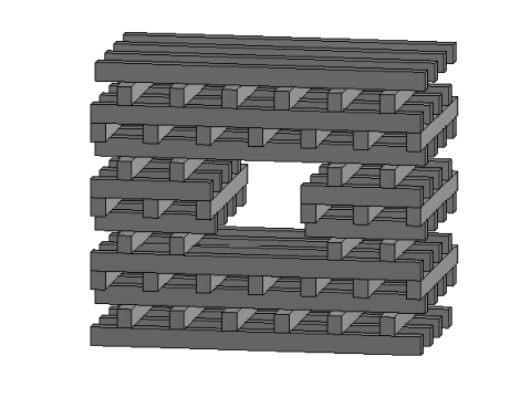
This waveguide supports an accelerating mode, that is, a mode with speed-of-light phase velocity and nonzero longitudinal field on axis. For this mode, , so setting determines . The accelerating field is shown in the left plot of Fig. 3.6.
Examining the fields, we find that there is a vertical deflecting field, shown in the right plot, with magnitude comparable to the accelerating field. This is due to the fact that the structure is not vertically symmetric. In fact, this is an inherent property of the photonic crystal: The lattice geometry itself is not symmetric under reflection across any plane perpendicular to the axis.
However, the structure is symmetric under the transformation of reflection in followed by translation of half a period in . Because of this symmetry, these vertical deflection fields average to zero over a lattice period, so particles will see no net deflection. Rather, they will see an undulator field with a period equal to the lattice period of 588 nm. The transverse fields on axis will cause energy loss due to synchrotron radiation. Since synchrotron loss scales as with beam energy , the loss will be significant at sufficiently high energies.
In examining the synchrotron loss in this structure, let us assume an accelerating gradient on axis of . While it is unlikely based on the damage threshold studies presented in Section 4.1 that such a gradient is achievable in silicon at 1550 nm, other materials and wavelengths may allow such high fields. Therefore this gradient value should be taken only as an example used to examine synchrotron loss, not as the breakdown limit of the structure.
In a high-energy collider, an accelerating field of 1 GeV/m will result in average incoherent synchrotron radiation loss of for 0.5 TeV electrons. Therefore this structure would not be appropriate for use in a high-energy linear collider. To overcome this problem, we must make the structure symmetric in both transverse dimensions to suppress dipole fields.
Although it might be tempting to consider this structure as a micro-period undulator for a radiation source, the extremely short period, together with the field strength limitation, leads to such a low undulator parameter that the photon yield would be insignificant. For instance, even if the fields were strong enough that peak vertical force were , the undulator parameter [20] would then be
The undulator parameter is a general measure of transverse field strength. An undulator causes a peak angular deviation of , where is the Lorentz factor. In this case, is several orders of magnitude smaller than in typical radiation devices, where . The number of photons per electron per period is , so only with large amounts of charge propagating for meters within the structure would result in significant photon yield.
3.3 Mode in symmetric structure
In order to make the structure vertically symmetric, we invert the upper half of the lattice so it is a vertical reflection of the lower half. The geometry, with a defect waveguide introduced, is shown schematically in Fig. 3.7 and visually in Fig. 3.8.


The inversion of half the lattice introduces a planar defect where the two halves meet, but this waveguide still supports a confined accelerating mode. Indeed, the mode is lossless to within the tolerance of the calculation, placing an upper bound on the loss of 0.48 dB/cm. Its fields are shown in Fig. 3.9; the computations are described in Secs. A.3 and A.4.

In this case the dipole fields are suppressed by the vertical symmetry of the structure. For this mode , so using a 1550 nm source determines . The individual rods are then 159 nm wide by 201 nm tall.
We can now explore the performance of this structure, according to the parameters defined in Sec. 1.4. First, the damage impedance is 6.10 Ω. Damage threshold measurements of silicon, described in Sec. 4.1, have shown a maximum sustainable energy density of at and 1 ps FWHM pulse width, resulting in an unloaded accelerating gradient of 221 MV/m. Further measurements have suggested that higher gradients could be achieved at longer wavelengths and shorter pulse widths, but that GeV/m acceleration is unlikely in silicon for near-infrared pulses.
Second, we examine the efficiency of the woodpile structure. The phenomena which determine the efficiency are described in Sec. 1.3. The efficiency depends not only on the electromagnetic mode itself, but also on the beam being accelerated. Now, we quantitatively compute the efficiency, and the characteristics of the particle beam needed to optimize the efficiency, following the treatment in [8]. For this mode the characteristic impedance is and the group velocity is . As described in Sec. 1.4, the Čerenkov impedance can be estimated from the characteristic radius of the waveguide. In our case the aperture is rectangular, so we define the parameter by , where is the aperture area. This yields .
With these parameters, we proceed to examine the efficiency of the structure using the same assumptions as in [8]. The accelerator segment is inside an optical cavity with a round-trip loss of 5%, and the external laser pulse is coupled into the cavity through a beamsplitter with reflectivity . We consider a train of optical bunches, each with the same charge, and assume that the duration of the train is much less than the slippage time between the particles and the laser pulse inside the structure. We also assume that , where is the laser pulse duration.
As described in Sec. 1.3, trying to accelerate too much charge can reduce the efficiency of an accelerator due to wakefield effects. Therefore, for a given and , the structure has a maximum efficiency . For each , we choose to maximize . These optimum values are plotted in Fig. 3.10.
From this we see that the efficiency can be made quite high. Even with just a single bunch, the efficiency reaches 37%, while for a train of 100 bunches, the efficiency is 76%. Once the optimum is computed for each , the total train charge and external laser pulse amplitude are chosen so that they together satisfy two conditions: First, that the peak unloaded gradient is equal to the maximum sustainable gradient in the structure, which we take to be 221 MV/m from the above discussion. Second, we require that the charge maximize the efficiency. We plot the optimum charge as a function of the number of bunches in Fig. 3.11.
As expected from the results in [8], the optimum total charge is low, only 1.17 fC for a single bunch and 10.3 fC for 100 bunches. With the charge having been computed, we can then find the average unloaded gradient for each . We can also compute the induced energy spread on the beam as the difference between the average accelerating gradient experienced by the first and last bunches in the train, relative to the average unloaded gradient. These quantities are plotted in Fig. 3.12.
From this plot we see that wakefields have a serious effect on the acceleration. For just a single bunch, the average unloaded gradient is reduced from 160 MV/m (which is reduced from 221 MV/m due to the advancement of the electrons with respect to the Gaussian laser pulse envelope) to 145 MV/m. The minimum at around 7 optical bunches is due to two competing effects. First, as the number of bunches increases from the single-bunch case, the total charge increases, generating more wakefields which are recycled within the cavity. But we see from Fig. 3.10 that as the number of bunches increases, the reflectivity decreases, so a smaller fraction of these wakefields are recycled. More concerning is the effect on the energy spread of the beam. Even with only two bunches, the spread in gradient is 6.1%, and with 5 bunches, the spread is 16.3%.
3.4 Coupling
A significant advantage of planar structures which are amenable to lithography is that a coupler from a laser source to the accelerating waveguide can be integrated with the rest of the structure as part of the same manufacturing process. While investigation of such couplers is currently underway, several possibilities have arisen. For a future accelerator we desire a coupler that is both efficient and compact. Because we wish to improve the overall optical-to-beam efficiency by recycling the laser power in an optical cavity as described in Sec. 3.3, avoiding coupling losses is essential to the efficiency of the accelerator. A compact coupler is desirable because any space that is used for coupling is not used for acceleration, so larger couplers reduce the average accelerating gradient. For the time being however, we have the simpler intermediate goal of a coupler that has sufficient efficiency for use in a proof-of-principle experiment, given that the input fields are limited by the damage threshold of the material. We have developed several preliminary ideas that might meet this goal.
The first possibility is simply to attempt to couple directly into the accelerating waveguide from a free-space laser mode. To investigate this, we used the finite-difference time-domain (FDTD) technique (see Sec. A.2) to simulate the reverse problem of radiation from the woodpile waveguide described in Sec. 3.3. We launch the computed woodpile mode down a 10-period waveguide segment using the total-field/scattered-field method, with the incident plane being immediately after the first period. The ends of the waveguide are open to free space, and the simulation space is surrounded by a uniaxial perfectly-matched layer. To reduce computational effort, we exploit the four-fold symmetry of the structure by placing magnetic boundaries at the and planes. We launch the mode as a continuous excitation, with a gradual buildup in the form of an error-function envelope in order to reduce the bandwidth. Some of the power is reflected at the end of the waveguide; some of the reflected power is also reflected at the beginning of the waveguide. We therefore monitor at a point in the center of the waveguide and continue the simulation until the amplitude at that point reaches steady-state. We then record the fields at points one quarter period separated in time to reconstruct the complex field amplitudes. We fit the component on axis over one period to a sum of forward- and backward-going accelerating modes. The ratio of the backward power to the forward power gives us the reflection coefficient for the exit of the waveguide. A plot of the fields for this simulation is shown in Fig. 3.13.
We find that only 7% of the power is reflected at the exit of the guide, indicating that the guide is well-matched to free space.
The reflection coefficient depends on the longitudinal position within a period at which the waveguide is cut. To compute this dependence, we repeat the simulation, varying the longitudinal position of the end of the waveguide. The transmission from the waveguide to free space remains quite high regardless of the end position. The transmission coefficients are plotted in Fig. 3.14; we see that in all cases the transmission is above 90%.
This is an encouraging result which suggests that we can couple a significant fraction of the energy in a free-space pulse into the waveguide. To develop this idea further, one could take a Fourier decomposition of the fields several wavelengths beyond the exit of the guide to find the far-field mode pattern. Then, one would determine the field pattern of a free-space mode which matches that far-field pattern as closely as possible while still being obtainable from a laser source and the available optical transport. By simulating, using the same technique, the propagation of that mode into the guide, one could determine the coupling efficiency from free space.
Another possible coupler involves using two identical accelerating waveguides placed parallel to one another and offset by several wavelengths, as has been explored for photonic crystal fibers [21, 22]. Because of the symmetry of such a structure the eigenmodes are the even and odd modes, which we denote by and respectively. We can choose the phases of these modes so that the accelerating mode in a single guide is very well approximated by the sum or difference of the eigenmodes. We therefore let
then and approximate accelerating modes in the left- and right-hand guides respectively. For a fixed frequency, the even and odd eigenmodes have longitudinal wavenumbers which we denote and respectively.
Now suppose that an accelerating mode is coupled into the left-hand waveguide. After a propagation distance , the state in the waveguide will be
If we let be half of the beat wavelength between the two modes,
we have that after propagating for distance,
Thus after half a beat wavelength, the mode transitions entirely from one waveguide to the other. This would allow one to butt-couple the mode to one waveguide, and run the particle beam through the other.
A simulation of this scheme is shown in Fig. 3.15.


In this structure, the waveguide centers are separated by 7 lattice periods, or 4.0 µm. We find that the beat length is , or 76.8 µm. We see from the figure that the fields are distorted due to the presence of the neighboring waveguide. The fields in each waveguide are not symmetric in as the fields shown in Fig. 3.9 are. There is a balancing act being performed here: If the waveguides are too far apart, they effectively act independently, so the mode wavenumbers are nearly equal and so the coupling length is very long. However, the coupling length cannot be made arbitrarily short, because if the waveguides are too close together, they will disturb each other’s fields, and the sum and difference states will no longer resemble accelerating modes. To develop this idea further, one could simulate this coupler design for a variety of waveguide separations. By finding the dependence on separation of both the beat wavelength and accelerator parameters such as the damage and characteristic impedances, one would be able to determine the suitability of this technique and optimize the separation.
Ultimately, we do require a coupler that is both compact and efficient, as remarked above. This might be accomplished by appropriately perturbing the geometry at a single position between the guides, as has been demonstrated for a two-dimensional photonic crystal waveguide [23]. There is also the possibility of coupling directly from a waveguide perpendicular to the accelerating guide, and this technique is currently under investigation at SLAC.
3.5 Particle beam dynamics
In Sec. 3.2 we found we had to adjust the geometry of the structure because of beam dynamics considerations, namely to suppress dipole fields. Here we examine the particle beam dynamics in this structure in more detail. Two concerns immediately arise. First, the structure has an extremely small aperture, approximately in each transverse dimension, so confining the beam within the waveguide presents a serious challenge. Second, since the structure is not azimuthally symmetric, particles out of phase with the accelerating field will experience transverse forces. As it turns out, an investigation of the second problem will yield insight into the first: The optical fields in the structure provide focusing forces which are quite strong compared to conventional quadrupole magnets and can be used to confine a beam within the waveguide. Therefore, we begin with a description of the transverse forces in the woodpile structure. We then propose a focusing scheme, and compute the requirements on the phase space extent of the particle beam.
In our analysis of the beam dynamics in this structure, we use the average of the fields over one longitudinal period of the photonic crystal waveguide. This is justified because the submicron period together with field intensities limited by damage threshold prohibits particles from acquiring relativistic momentum on the scale of a single period. To see this, one need only examine a normalized vector potential of the fields, defined by
where is the electric field magnitude. If , then the variation of a particle’s trajectory within a period is negligible, so the time-averaged force on the particle is well approximated by the force due to the longitudinally averaged fields. In our case, even for , . We therefore proceed to define the longitudinally-averaged fields, as seen by a speed-of-light particle beam. We take the fields to have time dependence, so that the real fields at spacetime coordinates are
We also define the phase of the fields so that a particle with trajectory experiences the peak accelerating field. The electric field experienced by such a particle is then
where is the Bloch wavenumber, since the fields have speed-of-light phase velocity. We can then define the averaged electric field by
and similarly the averaged magnetic field by
In order to better determine the nature of the forces a particle beam will experience, we now wish to decompose the fields within the waveguide into their azimuthal moments, that is, we wish to express each field component in the form
| (3.1) |
in polar coordinates. To perform this decomposition, we first notice that since the fields have speed-of-light phase velocity, each field component is harmonic in the transverse directions within the waveguide, satisfying
Let us now introduce the complex transverse coordinate
We can then consider the averaged fields as functions of . A result of complex analysis holds that any real harmonic function on an open, simply connected region is equal to the real part of an analytic function on [24]. It follows that within the waveguide region, we can represent a field component as , where and are analytic. Since an analytic function can be represented as a power series, we can write
for complex coefficients and . This forms a decomposition as desired in Eq. (3.1).
We can simplify the field expansions using the symmetries of the mode. We begin with the component. Let
Because of the even symmetry of the mode in the direction, we must have . Then
so . We then have
The accelerating mode also has even symmetry under a 180° rotation around the -axis. Since is a vector field, this means that . For , this means that
Thus for even. Finally, the system is symmetric under the composition of time reversal and reflection in . Under time reversal, and , so under the composition we have
Since we are choosing the phase of the fields so that an on-crest particle experiences peak acceleration, we have an even mode under this symmetry. Thus the components of the averaged fields are pure real, while the transverse components are pure imaginary. We can therefore write
for real coefficients .
We can similarly simplify the coefficients for . In this case, the even symmetry of the mode in the direction implies that . So if we now let
we must have . Then
As was the case for , here we must also have for even due to the rotational symmetry around the -axis. Again choosing the transverse field to be pure imaginary, we can write
for real coefficients .
Using the Maxwell equations, all the other field components are determined by , and can thus be specified in terms of the and coefficients. If we let , then it follows from the fact that in vacuum that
Thus the accelerating field on axis is given by .
The magnetic fields are then determined by the Maxwell curl equation , where is the impedance of free space, so that
The average transverse forces on a speed-of-light particle of charge moving parallel to the axis are given by the Lorentz force equation . We then have
and
Thus essentially forms a “potential” for the transverse force. Since satisfies , we have that , so that focusing in both transverse directions simultaneously is impossible. Indeed, let us compute the focusing gradients on axis: We have
Like in the case of a quadrupole magnet, we see here that the optical fields provide an equal and opposite focusing gradient in the two transverse dimensions. The coefficient specifies the strength of the optical quadrupole field. If we define the parameter
then particles of energy ahead in phase by will experience a focusing gradient in the direction, and a defocusing gradient in the direction, equal to
This is equivalent to a quadrupole magnet with gradient .
We now examine the implications of these forces for the structure we examined in Sec. 3.3. We first need to extract the and coefficients from the computed fields. We can express all the averaged field components within the waveguide in terms of these coefficients; the expressions for are given above, while for we have
Since all the fields are linear in the and coefficients, we perform a linear least-squares fit to the fields for and for . From this fit, we find that for the woodpile structure, we have . Thus for particles out of phase with the accelerating field by , experiencing peak transverse fields, the optical focusing force is equivalent to that of a quadrupole magnet with gradient, for accelerating fields at the damage threshold value of 221 MV/m.
We can now see directly the problem caused by the two concerns of small aperture and transverse forces in the structure. Particles which are out of phase with the accelerating field, even only slightly, will be defocused in one of the two transverse dimensions and rapidly driven out of the aperture. For instance, a particle just 10 mrad out of phase and 10 nm off axis will be driven out of the waveguide within 15 cm of propagation. Clearly a means of overcoming this obstacle is necessary for such an optical, azimuthally asymmetric structure to be viable as an accelerator.
We can in fact overcome the problem of transverse defocusing by altering the geometry of the structure to suppress the quadrupole component of the fields. To this end we adjust a single parameter of the structure geometry, namely, the removal or extension of the central bar a distance out of or into the waveguide, as shown in Fig. 3.16.

In order to avoid dipole fields we adjust ends of the bars on both sides of the waveguide symmetrically. We define the offset to be the distance the bars are removed from the guide, with a negative value describing extension into the guide. We can then examine the quadrupole field coefficient as a function of offset to see which offset value, if any, results in suppression of the quadrupole field. To this end we run mode computations with the geometry adjusted with a variety of offset values. We choose offset values to converge on the point with zero quadrupole coefficient to within the geometric resolution of the computation. This is shown in the solid blue curve of Fig. 3.17 (the other curves in the figure are discussed below).
We find that the quadrupole moment coefficient changes sign as the central bar is extended into the guide, so that suppression of the quadrupole field is possible by adjusting this parameter. Indeed, the quadrupole moment is suppressed by a factor of 57 with an offset of . The accelerating field for this structure geometry is shown in Fig. 3.18.

We notice that the field appears more symmetric under rotation by 90°, with the values increasing off axis equally in both transverse directions. It is also interesting to note that in this geometry the dimensions of the aperture are nearly equal in the two transverse directions. If we take the horizontal aperture to be the space between the central bars, then the horizontal and vertical apertures differ by only 0.2%. This suggests that despite the complex photonic crystal lattice geometry, the waveguide appears “square” to the fields. Finally, we note that for this mode, the damage impedance has increased from for the original mode to , improving the sustainable gradient to 301 MV/m.
By adjusting the geometry of the structure, we have addressed, at least to first order, our initial concern of transverse forces during acceleration. The small waveguide aperture remains a concern, but the above discussion of transverse forces presents a possible solution: Use the extraordinarily strong focusing forces available from the optical fields to confine the particle beam. We expect that stronger focusing forces will allow tighter confinement of the beam, and we now proceed to explore this idea quantitatively.
Since we have suppressed the focusing field in the accelerating structure, we must choose a different structure geometry for the focusing structure. While we could return to the original geometry which provided a focusing field, we now have the opportunity to adjust the central bar offset to optimize the structure for focusing. As we will see, nonlinear forces are responsible for instabilities in particle trajectories. Therefore we consider an optimal focusing mode to be one in which the lowest-order nonlinear field, in this case the octupole field due to the structure symmetries, is suppressed. Returning to Fig. 3.17, the dashed blue line represents the octupole field coefficient as a function of central bar offset, normalized to the accelerating field coefficient; its value is . We see from the dashed blue line that changes to the central bar offset fail to suppress the octupole moment in the accelerating mode. However, when the central bar is inserted into the waveguide by more than , a second mode appears which is qualitatively different from the first. The green lines in Fig. 3.17 show the quadrupole and octupole coefficients of this mode. From the dashed green line, we see that a appropriate central bar offset can suppress the octupole field of this mode. Indeed, for a central bar offset of , the octupole moment is suppressed by a factor of 26 relative to the original mode, while the quadrupole moment is enhanced by a factor of 3.2. The accelerating field for this structure geometry is shown in Fig. 3.19.

We have now found suitable optical modes for acceleration and focusing. The parameters of these modes, as well as the original mode, are shown in Table 3.1, with one final minor adjustment: Since the finite spatial resolution of the mode computation prevented us from finding an accelerating mode with the quadrupole moment entirely suppressed, we interpolate to find the parameters of the “ideal” accelerating mode with quadrupole coefficient identically zero. We do this by linearly interpolating the mode parameters, including multipole coefficients, offset, , and damage impedance, between the mode with the smallest positive quadrupole coefficient and the mode with the smallest negative coefficient. We similarly interpolate to find the focusing mode with zero octupole coefficient.
| Mode | Original mode | Accelerating mode | Focusing mode |
|---|---|---|---|
| Central bar offset | 0 | ||
| Quadrupole coefficient | |||
| 0 | |||
| Octupole coefficient | |||
| 1.100 | 1.689 | 0 | |
| Damage impedance |
With these parameters for the accelerating and focusing modes, we can now describe a system of focusing elements designed to confine the particle beam. We consider a focusing-defocusing (F0D0) lattice11 1 For the remainder of this section, we refer to the F0D0 lattice as simply the “lattice,” not to be confused with the photonic crystal lattice., in which each cell consists of a focusing segment of length run behind in phase for focusing in the direction, followed by a an accelerating segment of length , a focusing segment of length run behind in phase for defocusing in the direction, and then another accelerating segment of length [25]. We are free to choose the parameters and . Let be the peak focusing gradient for the focusing segment, given by , where is the energy of the ideal particle. If , then the thin lens approximation applies and we can consider the focusing and defocusing segments as lenses with focal lengths and , respectively, where . In that case, the betatron phase advance per half cell is given by . In addition, the maximum value of the function, which occurs at the midpoint of the focusing segment, is
The maximum value is an important parameter of a lattice because the RMS transverse size of a beam with geometric emittance is , so the maximum spot size over a lattice period is . The emittance must then be small enough that is several times less than the waveguide aperture.
We are now faced with a trade-off. By increasing , we can shorten the focal length and thereby reduce . Since the same maximum spot size can then be reached with a larger emittance, this loosens the emittance requirement on the particle beam. However, assuming is held constant, we have that , so that is reduced. Then a smaller fraction of the accelerator length is devoted to acceleration as opposed to focusing, so that the average gradient is reduced.
Let us assume an initial ideal particle energy of 1 GeV. Then if we run the focusing structure at damage threshold (with an on-axis accelerating gradient of 133 MV/m), we have . For our lattice we choose , which gives . We also choose ; then . The maximum beta function value is then , the length of the unit cell is , and the betatron period is . Note that the need to integrate both focusing and accelerating segments imposes no additional fabrication burden: Since the group velocity slippage of a laser pulse with respect to a luminal particle beam over a distance is 4 ps, coupling structures will need to be integrated on a length scale shorter than the smallest F0D0 lattice feature in any case.
The lattice described in the previous paragraph is stable under linear betatron motion. However, nonlinear transverse forces in the accelerating and focusing modes may cause instabilities which limit the dynamic aperture of the lattice and constrain the allowable emittance of the particle beam. To determine the effect of these forces and compute the required emittance of a particle beam, we perform full simulations of particle trajectories. These simulations include the dynamics of the particles in all six phase-space coordinates, with field values taken from the fit and coefficients. Note that the structure lengths are appropriately scaled to the ideal particle energy. Since is not constant, neither is , and both and are proportional to . The simulation techniques are described in detail in Sec. A.5.
To compute the dynamic aperture of the lattice, we simulate particles with initial positions uniformly distributed throughout the waveguide aperture. The initial transverse momenta of the particles are taken to be 0, as are the initial deviations of the particle energies from the ideal case. We first simulate particles which are exactly on crest initially. We propagate the particles for 3 m through the lattice and record whether or not each particle collides with the waveguide edge. The initial particle positions, color-coded as to the particle’s survival, is shown in Fig. 3.20.
In that figure, a red marker indicates that a particle initially at that position exited the waveguide aperture within 1 m of propagation. A green marker indicates that it remained within the waveguide through 1 m, but exited before 3 m, while a blue marker indicates that the particle remained in the waveguide through all 3 m of propagation. We see from the plot that most particles that are driven out of the waveguide exited within the first meter. The initial energy of the particles is 1 GeV, and after 3 m the energy of the ideal particle is 1.87 GeV. The ellipse indicated in the figure is the ellipse of largest area which still contains only particles which remain in the waveguide. If we take this ellipse to be the boundary of the particle distribution, we can use the relation to obtain the emittance requirement of the lattice. We find invariant emittances of
While these emittances are several orders of magnitude smaller than those produced by conventional RF injectors, because of the small bunch charge as discussed in Sec. 3.3, the transverse brightness (charge per phase space area) required in the optical structure is similar to that of conventional accelerators.
We can also examine the beam dynamics for particles which are slightly out of phase with the crest of the accelerating laser field. Running the same simulation as above, but with the particles given an initial phase offset, we find that the dynamic aperture is reduced as particles become further out of phase. This is shown in Fig. 3.21.

For particles ahead in phase (), we can see in the plots a pattern characteristic of a fourth-order resonance, indicating that the octupole field in the accelerating structure becomes significant as particles become off-crest. The difference in aperture shape between positive and negative phase shifts could be attributed to the sign difference of that octupole field.
With simulations of the dynamic aperture of the lattice for both on- and off-crest particles, we can now compute the dynamics of a realistic particle bunch, with variation in all six phase space coordinates. We take the initial transverse emittances to be those computed above for on-crest particles,
We also take the RMS phase spread and relative beam energy deviation to be and , respectively. We track the ensemble of particles for 3 m of propagation, as before, and record the phase space coordinates every 10 cm. We find that 261 of the 13228 particles simulated, or 2.0%, exited the waveguide before completing the 3 m propagation. From the recorded phase space coordinates we can track the invariant emittances as a function of propagated distance. The transverse emittances are shown in Fig. 3.22.
We see that the emittances increase initially, but that this increase slows as the propagation continues. For the full 3 m increases by 10.1%, while grows by 7.3%. Thus the growth in invariant emittance is much smaller than the energy gain, so that the geometric emittance of the beam will still be adiabatically damped. This shows that particle bunches can be propagated stably in a photonic crystal accelerator without an extraordinary enhancement to beam brightness.
Chapter 4 Woodpile materials and fabrication
In Ch. 3 we presented detailed simulations of a photonic accelerator structure, exploring several aspects of its operation. Bringing this type of structure from computer model to experimental reality involves several unique, difficult, and interrelated challenges, however. In this chapter we describe two of those challenges, namely the choice of material and the fabrication of the structure.
In the simulations presented in Ch. 3, we used silicon as the model for our material parameters. We made this choice because silicon has several properties making it a very attractive material for structure-based laser-driven acceleration. It is transparent in the mid-infrared [13], in particular in the telecommunications band at 1550 nm where many promising sources exist (see for instance [12]). It has a high index of refraction at those wavelengths, allowing for the complete photonic bandgap modeled in Sec. 3.1. It is highly resistant to ionizing radiation damage [26]. In addition, well-developed microfabrication techniques exist for silicon due to its use in integrated circuits. In Sec. 4.1 we explore in detail the suitability of silicon as an accelerator material with respect to the key parameter of the optical breakdown threshold.
While advanced fabrication tools and techniques exist for creating microstructures, the technology may not yet be available to manufacture optical accelerator structures with adequate precision. In Sec. 4.2, we describe some possible fabrication processes and the implications for choice of material. We then quantify the required fabrication tolerance of the woodpile structure in Sec. 4.3 by investigating the effect of layer-to-layer misalignment on the accelerating mode.
4.1 Damage threshold studies
As mentioned in Sec. 1.4, the accelerating gradient in a structure is ultimately limited by damage to the material. The value of this threshold, which is a function of wavelength and pulse duration, therefore has an overriding influence on the choice of structure material and laser source. It would then be highly informative, as we embark on an exploration of structure-based optical acceleration, to have a comprehensive set of damage threshold data for a variety of materials and full range of laser pulse parameters. Such knowledge does not exist. However, a significant amount of research has taken place on optical damage of a few materials, so that theoretical descriptions of dielectric breakdown have been developed. We discuss the prevailing theories behind the optical breakdown process and their implications for accelerators in the next subsection. Then we will describe an experiment to measure the optical breakdown threshold of crystalline silicon for ultrafast pulses in the infrared and present the results.
4.1.1 Theoretical background
As discussed in [27], optical breakdown in dielectric materials occurs in four general steps: (1) Seed conduction electrons are generated by photoionization, (2) they are accelerated in the laser field and generate an avalanche by impact ionization, (3) the laser pulse heats the resulting plasma, and (4) the electron energy is transferred to the lattice, resulting in ablation. This schematic description raises an important question: To what extent do multiphoton effects drive the photoionization process? According to the Keldysh theory of photoionization [28], there are two limiting cases. For long wavelengths and strong fields, the phenomenon becomes that of tunnel ionization (TI), in which the field reduces the Coulomb barrier sufficiently for a valence electron to tunnel through it. In that case the ionization rate depends only weakly on the wavelength. In the other extreme, for shorter wavelengths and weaker fields, the phenomenon becomes that of multiphoton ionization (MPI), in which the energy of several incident photons ionizes an electron. In that case the ionization rate depends strongly on the photon energy and hence the wavelength. As a practical matter for accelerator structure design, can we significantly increase the damage threshold by lengthening the wavelength beyond a multiphoton threshold? For instance, the bandgap of silicon at room temperature is 1.12 eV, corresponding to a free-space wavelength of 1107 nm. By using a wavelength longer than 1107 nm, in the multiphoton regime seed electrons can only be generated by two-photon absorption, which has a much lower cross-section than single-photon absorption. Similarly, operating at wavelengths beyond the two-photon threshold at 2214 nm might yield a further increase in sustainable gradient.
The experiments described in [27] were conducted at a wavelength of 800 nm on fused silica (bandgap energy , requiring six-photon absorption) and barium aluminum borosilicate (BBS, , requiring three-photon absorption). The authors reached the conclusion that multiphoton ionization dominates as the seed process for FWHM pulse widths , while tunneling dominates for shorter pulses. Other experiments which have been conducted at 527 nm and 1053 nm are consistent with this conclusion [7]. However, another experiment measuring breakdown thresholds as a function of polarization has called into question the significance of MPI in the breakdown process [29]. In that study the authors showed that breakdown thresholds were independent of polarization, and argued that the inefficiency of circularly-polarized light for MPI indicates that MPI is not the dominant process. Also, evidence indicates that TI is the dominant ionization process in the mid-infrared [30]. Therefore, we may not be able to arbitrarily increase the sustainable gradient by using longer wavelengths.
4.1.2 Experimental setup and procedure
As samples for the damage study, we used undoped crystalline silicon cut from a wafer with a (100) surface orientation. We conducted experiments starting at and extending longer in wavelength beyond 2200 nm. The pulse widths varied between 0.66 and 1.12 ps, depending on wavelength.
This was a pump-probe measurement in which a CW helium-neon laser was focused on the same spot on the sample as the infrared pulses and damage was detected by observing a decrease in reflected HeNe intensity. A schematic of the experiment is shown in Fig. 4.1.
The experiment included the diagnostics necessary to measure both the pulse energy and the extent of the pulse in all three spatial dimensions, in order to obtain the energy density. We also measured the spectral content of the pulse to confirm that no residual light at shorter wavelengths was present.
The infrared pulses were generated by a commercial Spectra-Physics OPA-800 optical parametric amplifier (OPA) pumped by a Ti:sapphire laser system. The OPA produced pulses with energy at a repetition rate of 240 Hz; the experiment detected multiple-shot damage. The pulses first passed through a neutral density filter to control the intensity. They then passed through several diagnostic pellicle beam samplers. The first of these directed a small fraction of the pulse energy into a pyroelectric detector that served as the main pulse energy diagnostic. An off-axis parabolic mirror was used to focus the pulse just enough to ensure that all the energy was captured by the detector. The second beam pick-off directed a small amount of the pulse energy into a multimode fiber. This was connected to an InGaAs photodiode to optimally align the fiber, and then to an optical spectrum analyzer (OSA) to measure the spectrum.
After the diagnostic pick-offs the pulses were directed by a flip mirror toward the sample. They were normally incident on the sample, focused by a CaF lens to minimize dispersion, while the HeNe beam was incident at an angle. The sample was mounted vertically on motorized translation stages with motion in the plane of the sample, and was oriented during initial setup so that it was parallel to the directions of motion of the stages. Razor blades were mounted in the same plane as the sample to conduct knife-edge transverse spot size measurements. A photograph of the setup is shown in Fig. 4.2.

With the flip mirror down, the pulses would proceed to an autocorrelator setup used for measuring the pulse duration. A schematic of the autocorrelator is shown in Fig. 4.3.
The infrared pulses were split into two arms of an interferometer with a pellicle beamsplitter, and one arm had an adjustable delay. After passing through their respective paths, the beams were directed parallel to one another and then into an off-axis parabolic mirror. This focused and crossed the beams at the same position on a nonlinear barium borate (BBO) crystal, which was mounted on a rotation stage to adjust the angle of its optic axis. At the proper angle, pulses of double the frequency (shown in blue in Fig. 4.3) were produced between the two crossed beams, as long as the pulses were coincident on the crystal. A beam sampler was used to direct some of the doubled light onto a CCD to optimize the alignment. The remainder was captured by a photodiode, whose signal was integrated in a Stanford Research Systems SR250 gated integrator, and then passed to the data acquisition system (DAQ) for recording. We obtained an autocorrelation trace by varying the delay in one arm of the interferometer, and thus the temporal overlap of the beams on the crystal, and observing the resulting signal on the diode. A picture of the autocorrelator is shown in Fig. 4.4.

Our data acquisition system consisted of a Dell Precision 330 computer with a 1.8 GHz Pentium 4 processor and 1 GB RAM. It contained a Newport ESP6000 motion controller card and a National Instruments PCI-MIO-16E-4 data acquisition board. The motion controller was used to move, and read back position data from, the translation stages on which the sample was mounted. The DAQ board was used to acquire analog voltage data from the pyroelectric detectors and photodiodes, as well as control a motorized flipper used as a beam stop to begin and end sets of damage data. LabVIEW software was used to automate the data taking and perform initial processing of the data. Our pyroelectric detectors output signals on the time scale of 100 µs, slow enough so that an entire trace could be captured by the 100 kHz ADCs in the DAQ board. The signal level was taken to be the maximum value of the pyro voltage during the trace.
For each wavelength tested, we first measured the spectral content of the pulses to confirm the absence of shorter wavelength light. Such light could have come from the Ti:sapphire pump at 800 nm, the signal wavelength when the idler was desired, or in the visible range from the pump mixed with the signal or the idler within the OPA. The beam was coupled via fiber to an optical spectrum analyzer (OSA). We first acquired a spectrum over the entire 600–1700 nm range of the OSA; a sample spectrum from a 1550 nm run is shown in Fig. 4.5.
The noise floor in the spectrum shown is determined by the sensitivity of the OSA. For higher sensitivity, we also acquired spectra over smaller ranges centered on wavelengths where shorter-wavelength contamination might have been present. Since we expect that such contamination would have been narrow-band, centered only at the wavelengths of light produced within the OPA, this was sufficient to confirm the absence of additional wavelengths in the pulses. In each case we verified that the level of any shorter wavelength light was at least 30 dB less than the wavelength of interest.
Next, we took an autocorrelation trace to measure the pulse duration. We adjusted the delay arm of the autocorrelator in a pseudorandom sequence in order to prevent slow pulse energy drifts from causing a systematic error. While the delay stage was manual, the DAQ prompted the user to set each delay at the proper micrometer reading in order to form the pseudorandom sequence. For each delay, we acquired diode levels for 1000 shots. We then fit the data to an autocorrelation profile, assuming a temporal profile of the incident pulse, as is the case for passively modelocked lasers [5]. The autocorrelation trace for the 1550 nm run, along with the fit, is shown in Fig. 4.6.
From the fit we deduce a FWHM pulse duration of .
After the autocorrelation trace was taken, the final focus lens was adjusted to place the beam waist just in front of the sample surface. This was to ensure that maximum fluence occurred on the sample surface rather than in the bulk, so that the transverse spot-size measurements would yield relevant results. Also, the HeNe beam was spatially overlapped with the infrared pulses and one damage spot was created to confirm that the pulse energy was sufficient and the focus was tight enough for damage to occur. Once this was complete, the transverse spot sizes were measured using the knife-edge technique. This was accomplished using razor blades glued to the same microscope slide as the silicon sample so that their edges were in the same plane as the sample surface. The platform holding the sample and the razor blades was mounted on a pair of Newport M-UTM150CC1DD motorized linear stages to allow for motion in both directions in the plane of the sample. A Molectron P1-45 pyroelectric detector was placed behind the knife edges to capture any unblocked light. A LabVIEW VI was used to automatically move the stages, in one dimension at a time, to adjust the position of a knife edge in pseudorandom order. At each position, we acquired pyro signal levels for 1000 shots. The horizontal knife edge measurement for the 1550 nm run is shown in Fig. 4.7.
We fit the data to an error function, which is the curve that results from integrating a Gaussian spot intensity profile. For this knife-edge scan, we acquire a spot width of .
As a final setup step, we calibrated the sensitive pyroelectric detector used to measure pulse energy, also a Molectron P1-45. This was necessary for each wavelength because the reflectivity of the pellicle beam sampler varied with wavelength. We calibrated the Molectron detector against an Ophir Optronics PE10 energy detector; since the Ophir detector had an absolute calibration in our wavelength range, this allowed us to have an absolute calibration of the Molectron detector at each wavelength. We placed the Ophir detector behind the sample and used the stages to remove the sample from the beam path. This ensured that the Ophir detector was reading the pulse energies after the beam passed through its transport through the sample and therefore was measuring the actual incident pulse energies. We acquired approximately 1200 shots on both the Ophir detector and the Molectron sensor for a range of energies. A linear fit was then performed to obtain the calibration.
4.1.3 Data analysis and results
Once the setup was complete for a particular wavelength, damage data were taken. For each event, the pulses were allowed to illuminate the sample by removing a beam stop, and infrared pulse energy and reflected HeNe power were then acquired on a shot-to-shot basis. Since the data acquisition rate was limited to , less than the repetition rate of the laser, not all samples were acquired. The acquisition was stopped, and the beam stop reinserted, when either the HeNe power decreased, indicating damage, or a certain amount of time, usually , had elapsed with no damage. Each set of pulse energy and HeNe power data, taken between the time the beam stop was initially removed and the time the acquisition was stopped, constituted one “event.” Events were taken both above and below the damage threshold, and the sample was moved at least 1 mm between each event to avoid geometric deformities from one damage spot affecting subsequent measurements.
A sample event is plotted in Fig. 4.8.
We notice that the reflected HeNe power increases for a fraction of a second before falling off. This is ostensibly due to additional focusing from the silicon surface as the damage morphology develops. Indeed, we observed using a CCD image of the reflected HeNe light that the mode pattern changes for about a second during damage before finally disappearing.
From the multiple-shot data in this event and others like it, it is not immediately clear how to compute the measured damage threshold. We assume that damage was initiated by a single pulse, with further damage occurring in each subsequent shot due to the field enhancement resulting from the initial deformation of the surface. That pulse may or may not have been acquired, and the data do not tell us how long before the visible onset of damage the pulse occurred. However, we can make a maximum likelihood estimate for the damage threshold based on a few assumptions. First, the damage process is deterministic, as reported in [29], so damage did occur after a pulse that exceeded the threshold and did not otherwise. Second, at least one pulse with energy above threshold therefore must have occurred within the 1000 acquired shots before the visible onset of damage. Third, no such shot occurred more than 1000 shots before the visible onset of damage, or more than 1000 shots before the end of an event in which no damage was observed.
Using these assumptions, we form a maximum likelihood estimate of the damage threshold as follows. The data for each event include a sequence of acquired pulse energies, , as well as a sequence of reflected HeNe diode voltages acquired simultaneously. If damage occurred during the event, we define the “damage index” to be the index of the first shot in which the reflected HeNe diode read more than below the initial reading at the start of the event. We then divide the event into “blocks” of 1000 acquired events as follows: If damage occurred, we have assumed that the shot that initiated it occurred within the 1000 acquired shots before . The index of the last shot where we know damage did not occur is therefore . If , then there is no shot we can be sure did not cause damage. We call the set of pulse energies the “damage block.” We then divide the acquired pulse energies which we know did not cause damage into “no-damage blocks” of 1000 pulses each, starting with the first acquired pulse. If no damage occurred during the event, we let ; then regardless of whether damage occurred there are no-damage blocks in the event.
Because we did not acquire the energy of each incident pulse, we do not use the acquired pulse energies directly to form our damage threshold estimate. Rather, we use the acquired pulse energies to form a statistical description of each block, and use those statistical parameters to estimate the threshold. To obtain the number of incident pulses in a block, we need to know the ratio of incident to acquired pulses. The DAQ records the total elapsed time for the event; then for the known laser repetition rate we have . For each block , we fit the pulse energies in that block to an asymmetric Gaussian distribution, with peak and RMS widths and for and respectively. We ignore the pulse energies with , and consider the distribution of pulse energies in a block to be a one-sided Gaussian with peak and RMS width . We can justify this because if damage occurred, it is unlikely that it was a pulse with such low energy that caused it, when pulses with higher energies were present. Conversely, if damage did not occur, the fact that a relatively low-energy pulse did not cause damage yields little information. The probability density function for pulse energy within block is therefore
| (4.1) |
We estimate the number of relevant incident pulses within the block to be .
We can now form a likelihood function from these statistical parameters. For a given block , let be the probability that a single incident pulse from block does not cause damage if the pulse energy damage threshold is . This is the probability that a pulse energy . From Eq. (4.1) we have that if , and that for ,
Then the probability that no damage occurs within the block is the probability that none of the incident pulses initiate damage, or
This equation makes physical sense, since not only is damage more likely to occur if the mean pulse energy is increased, it is also more likely to occur if the pulse energy jitter increases. Increased jitter makes it more likely that there will be a pulse above damage threshold, underscoring the importance of stable laser sources for accelerator applications.
To compute the likelihood function we use all the blocks acquired during the course of a run at the given wavelength. Let be the collection of damage blocks for the run, and let be the collection of no-damage blocks. Our likelihood function is then
To find the value of with maximum likelihood, we compute the negative log likelihood, given by the function
We compute the function numerically, and use the matlab minimization routine fminbnd to find the value of which minimizes as well as the minimum value . We then use the routine fzero to find the pulse energies and above and below , respectively, for which , and defined the error on to be . For instance, for the run at , the threshold was .
We now have the information required to reconstruct the damage threshold energy density in the material. For a pulse with peak intensity , the energy density inside the material is given by
where is the index of refraction; the factor of takes into account Fresnel reflection at the surface and the slower speed of light in the material. For our pulses we have assumed an intensity distribution in space and time given by
and obtained fits to the parameters , , and from our knife-edge and autocorrelation measurements. The total pulse energy is then , so we have as our damage threshold energy density
We obtained data sets for , 1700 nm, 1900 nm, 2100 nm, and 2256 nm. The damage threshold results are plotted in Fig. 4.9.
The data point at 2100 nm was repeated several months after the initial point was taken, in order to check the consistency of the setup; we found the two points to be within reasonable statistical error of one another. Because much of the damage literature gives damage threshold values in terms of the incident pulse fluence, we present those values as well here. The damage fluence is computed simply as and is plotted in Fig. 4.10.
Comparison among damage thresholds at different wavelengths is complicated by the fact that each measurement was taken using a different pulse duration. We can attempt to remove the pulse duration dependence using the empirical scaling law of reported in [31]. However, we should note that the result in [31] was determined for oxide thin films and might not be applicable to silicon. The damage energy density and fluence, normalized for pulses with 1 ps FWHM duration, are plotted in Fig. 4.11.
We first notice that the damage threshold of silicon at these wavelengths is low compared to larger-bandgap materials that have been previously measured. The normalized fluence thresholds of 160– are an order of magnitude lower than those for fused silica, CaF, and other fluorides reported in [7]. It is also several times lower than the thresholds for the larger-bandgap semiconductors ZnS and ZnSe reported in [30] for wavelengths of 400 and 800 nm and in the mid-infrared.
We also notice that the damage threshold does indeed increase as the wavelength approaches the two-photon absorption threshold, between 1700 nm to 1900 nm. This is reasonable, since we would not expect a sharp cutoff from an MPI-dominated process because silicon has an indirect bandgap. At wavelengths longer than 1900 nm, we then see a decrease in damage fluence. This may be due to the same mechanism as reported in [30], in which the damage threshold decreased at longer wavelengths because of the increased probability of tunnel ionization. Therefore, the increase in damage threshold from 1700 nm to 1900 nm is not dramatic enough to indicate that the damage process is highly dominated by the MPI effect. In addition, since the increase in threshold would only increase accelerating gradient by , the decision whether to use longer wavelengths outside the telecom band in an accelerator application might be guided by other considerations. And because of the low breakdown threshold overall, the choice of material remains an open question, which we discuss further in the next chapter.
4.2 Fabrication possibilities
A key consideration in the design of optical accelerators is the challenge of fabricating structures at optical length scales. It is beneficial to choose geometries which capitalize on the many microfabrication tools and techniques developed by the integrated circuit and MEMS industries. Indeed, the woodpile lattice stands out among several possible three-dimensional PBG lattices in that the methods of fabricating the lattice and defects within the lattice are relatively straightforward. Straightforward, to be sure, does not necessarily mean easy, or even possible. In fact, reliable, economical production of the structures described in Ch. 3 at wavelengths in the near infrared might not yet be possible. However, a number of promising methods for fabricating woodpile-based structures have been explored by the optics community, and great progress has been made. In this section we review some of these techniques. As the integrated circuit industry continues to develop methods and equipment for constructing geometries at ever-smaller feature sizes, we can expect that fabrication of woodpile-based optical accelerator structures will become viable.
The woodpile structure is amenable to established microfabrication techniques because of its layered structure. Each layer of a device can be constructed separately using a photolithographic process, and the structure built up layer by layer. Thus the fabrication process divides naturally into two parts, the construction of each layer and the composition of multiple layers into a working device. As we will see, the second part of the process presents a much greater challenge than the first.
The photolithography process generally takes place as follows [32]. It begins with a substrate in the form of a circular wafer of solid material, typically crystalline silicon, 100–300 mm in diameter, and several hundred microns thick. First, a thin film of the material to be patterned is deposited on the substrate. Then, liquid photoresist is placed on the wafer, which is then spun at high velocity to form a thin layer. Next, the wafer is selectively exposed to ultraviolet light by placing a mask between the UV source and the wafer, causing a chemical change in the photoresist in the areas exposed. The wafer is then immersed in a developer solution which removes the resist in the exposed areas (for a positive resist; negative resist behaves in the opposite manner). Finally, when the wafer is etched, the remaining resist protects the selected areas of the wafer from the etch process, resulting in a patterned layer. Equipment exists which enables efficient, cost-effective mass-production of patterned films.
The precision of photolithographic patterning is fundamentally limited by the wavelength of UV light used to expose the resist. The current generation of tools uses 193 nm light, which is greater than the rod width of a woodpile structure operating at 1550 nm. While state-of-the-art equipment can produce subwavelength features with sizes down to 30 nm, a highly complex imaging system is required [33]. However, a patterning method has been demonstrated which can accurately produce, with simpler equipment, layers of the woodpile structure with feature sizes well below the resist exposure wavelength. This technique, called “fillet processing,” is described in [34]. It proceeds by using adhered sidewalls from a thin film deposition as an etch mask, rather than using photoresist directly. First, a series of lines are created in SiO with period and width ; those features are large enough to be patterned with optical lithography. Then polysilicon is deposited over the SiO lines to form a layer of thickness on the entire surface, including the sidewalls. Next, the polysilicon is etched anisotropically to remove just the material adhered to the tops of the SiO lines and in the trenches between them, but not the sidewalls. The SiO is then dissolved, leaving only the pattern of polysilicon sidewalls, with width and period . Those sidewalls are used as an etch mask for the material beneath. Thus the width of the rods is controlled by the thickness of the deposited material, rather than by a photomask, overcoming the wavelength limitation of the feature size. The required etch depth does not pose a challenge, since the rod width and depth are and respectively, so the relevant aspect ratio of etch depth to width is less than . It is also possible to use electron-beam lithography to construct the small features of each layer, but that method is highly time consuming and therefore unsuited to mass production [35].
Previous investigations of woodpile structure fabrication have also explored different means of stacking the layers into a photonic crystal lattice. In [34], the structure is built up layer-by-layer on a single substrate. This is accomplished by filling the vacuum regions of each layer with SiO and planarizing in order to have a flat surface on which to construct the subsequent layer. When the final layer is completed, the entire structure is then wet-etched to remove the SiO. In [36], the wafer fusion technique was used, in which each layer is first constructed on a different wafer, and the layers are then bonded together and one of the substrates removed. This method is attractive because it allows all the photolithography steps for a single structure to occur in parallel.
Both methods of stacking individual woodpile layers into a structure present the considerable challenge of aligning the layers with respect to one another. In [34] and [36], the investigators were only interested in producing the woodpile lattice, so 4 or 8 layers were sufficient, and an adequate structure could be produced even with imprecise alignment. However, for a woodpile accelerator structure, 20–30 layers are necessary because there must be enough layers of PBG lattice to confine a mode, so a method of achieving highly precise alignment is required if woodpile-based accelerators are to be realized. The fillet processing method which reduces the feature sizes available from optical photolithography does not similarly improve the alignment precision. Both e-beam and state-of-the-art optical lithography are capable of reaching the alignment tolerances necessary to produce a working woodpile structure, but these methods are either highly complex or time consuming [37, 35]. There are more exotic techniques, such as interferometric alignment [38] and stacking by micromanipulation [39] which hold promise for efficient, cost-effective fabrication. However, alignment remains the most challenging aspect of woodpile structure fabrication, so in the next section we examine the effects of misalignment and evaluate the tolerances required.
4.3 Tolerance studies
To assess the effect of layer-to-layer misalignment in the woodpile structure, we perform a set of simulations of the structure, with the position of each layer randomly offset in the relevant horizontal directions: Longitudinal rods are displaced transversely, while the transverse crossbars are displaced longitudinally, and the crossbars in the waveguide layers are displaced transversely as well. Since we are studying the effect on the accelerating mode, we do not include angular misalignments: Angular misalignments would destroy the longitudinal periodicity of the structure, so we would in effect have a waveguide that slowly changes geometry with longitudinal position. This would result in scattering or radiative loss as the fields propagate down the waveguide, rather than a uniform alteration of the accelerating mode. The consequences of angular misalignments remain to be studied.
We choose an RMS offset of . We performed 20 simulations, each with different offsets, using the mpb iterative eigensolver described in Sec. A.1. Of these simulations, one failed to support any accelerating mode. For the others, we found the accelerating mode at the speed-of-light frequency of the perfectly aligned structure, as the source frequency will be fixed by the bunching of the particle beam. The key figure of merit for a misaligned structure is the relative wavenumber error, given by
where is the wavenumber of the speed-of-light mode in an ideal structure, and is the wavenumber of the accelerating mode in the misaligned structure. This is because if is too large, the fields will get out of phase by and become decelerating fields. A histogram of the relative wavenumber errors is shown in Fig. 4.12.
It is interesting to note that all but one of the wavenumber errors were positive. The cause of this is not clear, but may be related to the second-order nature of effect of the transverse misalignments. If we follow the perturbation technique prescribed in [40], we find that the first-order frequency shift from transverse horizontal displacements of the rods vanishes.
The fields will acquire a phase shift of relative to the particle beam after length . Let us consider a structure to be acceptable if , as this is the distance in which the laser pulse will slip by 1 ps with respect to the particle bunch, and is therefore the characteristic length of a structure segment. This requirement corresponds to . We find that 5 of the 20 simulated structures meet our requirement, giving a yield of 25%. This yield level is acceptable if we take advantage of economical mass-production techniques for silicon microstructures. We can therefore quote a misalignment tolerance of the woodpile structure of 25–30 nm.
Chapter 5 Toward a photonic crystal accelerator
In Ch. 3 we described a structure suitable for structure-based, laser-driven acceleration. Its parameters are as follows:
- •
The underlying photonic crystal is a woodpile lattice, as shown in Fig. 3.1. The rod spacing is , the rod width is , and the rod height is . For a wavelength of 1550 nm, this gives , , and . The lattice is constructed out of silicon with a relative permittivity of .
- •
- •
To improve particle beam stability in the structure, we modify the geometry to suppress unwanted azimuthal moments, as described in Sec. 3.5. We modify the structure by inserting the central bar into the waveguide, as shown in Fig. 3.16. We obtain two structures; one for acceleration and the other for focusing. For the accelerating structure, the bar is inserted into the guide; for the focusing structure, it is inserted .
- •
The accelerating structure can sustain an unloaded gradient of 301 MV/m at . Its characteristic impedance is and its group velocity is . Therefore a laser pulse will lag the particle beam by 1 ps after 100 µm of propagation, so that will set the length of each accelerating segment.
- •
Operated at damage threshold, the focusing structure has a focusing gradient equivalent to an 831 kT/m quadrupole magnet.
However, this is certainly not the only suitable photonic crystal accelerator structure. Indeed, there are many choices to be made to optimize the accelerator. These include not only the structure geometry, but also the dielectric material and laser source. In this chapter we consider some of these choices.
5.1 Materials and laser considerations
As we remarked in Ch. 4, silicon has several properties desirable for a photonic crystal accelerator structure. However, the damage threshold studies reported in that Chapter reveal that silicon can sustain an accelerating gradient of only at , improving to at longer wavelengths. We are therefore led to question whether silicon is the most appropriate material, and what some alternatives might be. As described in Sec. 4.1, our damage studies, combined with those in the literature, indicate that materials with wider electronic bandgaps have a higher breakdown threshold. However, this involves a trade-off: A lattice with a complete photonic bandgap generally requires a refractive index contrast [17], and high-index materials tend to have narrow electronic bandgaps. Silicon’s high index is ideal for photonic crystals but its narrow electronic bandgap yields a low damage threshold. On the other hand, fused silica, with an electronic bandgap and a high breakdown threshold [27], has a refractive index of only 1.44 at 1550 nm [41]. Other materials may strike a better balance between refractive index and electronic bandgap. Possible candidates are rutile (birefringent; , [42], bandgap [43]), diamond ( [44], [45]), and silicon carbide ( [46], [47]).
To determine whether these lower-index materials might be suitable for a photonic accelerator structure, we simulate a woodpile geometry based on diamond, the lowest-index material mentioned with at 1550 nm. The simulation proceeds similarly to that presented in Ch. 3, starting with the bandstructure computation. The first step is to optimize the rod width with respect to the lattice constant for maximal bandgap. We find that the optimum rod width occurs at . This lattice with the wider rods is shown in Fig. 5.1.

In that figure, the notation is the same as in Fig. 3.3, with Brillouin Zone points plotted in Fig. 3.2. While the bandgap is not as wide as with silicon, the diamond lattice does exhibit an omnidirectional bandgap, shown in yellow in Fig. 5.2, with width-to-center ratio of 5.4%.
Finally, we create a waveguide in this lattice and compute an accelerating mode. We use the same geometric parameters as in Sec. 3.3; namely, we take the waveguide to be wide by (7 layers) tall. We find that there is indeed an accelerating mode in this waveguide; the accelerating fields are plotted in Fig. 5.3.

However, we notice that in comparison with the mode in the silicon structure plotted in Fig. 3.9, there are significant fields which extend throughout the PBG lattice surrounding the waveguide. Therefore this mode is not as well confined as the mode in the silicon structure; indeed, instead of being radiatively lossless, it has a loss of 35.3 dB/cm. Its impedance and group velocity are also reduced, to and respectively. These effects are likely due to the mode frequency of being close to the bandgap edge, and might be reduced by perturbing the structure geometry slightly, as was done to affect the quadrupole fields in Sec. 3.5. More importantly, however, the damage impedance is only reduced slightly from the silicon case, to from . Therefore a gain in the damage threshold from an alternative material would be largely preserved in the sustainable gradient of the structure. For instance, suppose the damage threshold in diamond is 10 times higher than that of silicon. The damage field is then times higher. Then, since the sustainable gradient is proportional to , the slightly lower damage impedance for this mode only reduces the gain in sustainable gradient to a factor of 3.02.
This computation shows that larger-bandgap, lower-index materials could be suitable for a photonic accelerator, and possibly yield significant improvements in sustainable gradient. However, those improvements would need to be weighed against other advantages of silicon, such as ionizing radiation hardness, thermal conductivity, and amenability to microfabrication. For the future, a comprehensive study of damage thresholds and other material properties for a variety of dielectrics would serve to inform the choice of accelerator structure material.
Another possible mechanism for improving the damage threshold of an accelerator structure material is to change the laser wavelength. For operation in the near infrared, structures such as the one presented here are not limited by laser power availability. Even if a material were found that could sustain a 1 GeV/m acceleration gradient in the woodpile structure, the large characteristic impedance means that at 1550 nm the peak power required would be only . Such powers are readily available at high efficiencies from commercial fiber lasers; a system is even available which produces pulses with 2 MW peak power at a 60 kHz repetition rate [48]. However, because of the possible role of multiphoton ionization in the damage process, especially for wide-bandgap materials, lengthening the laser wavelength away from the near infrared may yield higher sustainable gradient. Efficient fiber sources exist in Er:glass at and Yb:glass at . Degenerate optical parametric generation pumped by these sources to double the wavelength would allow efficient generation of mid-infrared wavelengths, and an effort to accomplish this using LiNbO is underway [49]. Ultimately, the challenge of developing a mid-infrared source will need to be weighed against the potential gain in gradient as well as the alternative challenge of developing structures from higher-damage threshold materials.
5.2 Structure considerations
In addition to the choice of material and laser source, the geometry of the structure itself is open to alternative candidates. The most significant drawback to the woodpile geometry described in Ch. 3 is the difficulty of fabrication, as discussed in Ch. 4. Other geometries may be easier to fabricate by not requiring alignment of so many layers.
One possibility for simpler fabrication would be to return to the two-dimensional geometries presented in Ch. 2. As mentioned in that chapter, a method of vertical confinement is needed for these structures to be practical. We might therefore consider placing a finite slab of 2D structure between other structures which provide the vertical confinement. This is shown schematically in Fig. 5.4.

One proposal for vertical confinement calls for using bulk three-dimensional photonic crystals which can be assembled all at once, rather than layer by layer [50, 51]. There are several such photonic lattices. The inverse opal structure [52, 53] can be constructed by first creating a lattice of spheres by self-assembly, depositing a second dielectric, and dissolving the spheres. Another option is the square spiral array geometry [54, 55, 56], which is constructed by rotating the substrate during a deposition. While these 3D lattices can be fabricated economically, those same fabrication processes can not be used to incorporate waveguide structures; those are incorporated only in the two-dimensional slab.
An even simpler option would be to use a simple dielectric multilayer stack for vertical confinement, as proposed in [57]. This would involve only depositing thin films of different materials in an alternating pattern; no patterning of the films would be required. The thicknesses of the films would be chosen to provide the best vertical confinement; however this a nontrivial task because a dielectric multilayer does not exhibit a complete PBG.
In either case, the bandgap of the 2D and 3D structures would need to be properly matched to minimize leakage in the heterogeneous structure. This is complicated, since the bandstructure of the 2D slab depends on its placement within the vertically confining structure. In Ch. 2 we took the fields to be uniform in the vertical direction; in the Fourier domain this was equivalent to fixing . The 2D bandstructure, though, will be different for different values of , and a slab within a larger structure will exhibit a wide range of vertical spatial frequencies. If the 2D and 3D structures shared the same periodicity in the horizontal directions, the entire structure would then be periodic in both horizontal dimensions. It would therefore have a 2D bandstructure which we might optimize for widest bandgap.
Chapter 6 Conclusion
Significant improvement in accelerating gradient is necessary if accelerator-based particle physics is to continue its pace of discovery. While lasers can provide extraordinary energy density, the question remains of how to utilize properly the laser power to accelerate a charged particle beam.
Photonic crystals have great potential for use in accelerator structures. By being constructed out of dielectric materials alone, they can circumvent the problems of metals at optical frequencies. We have described a general procedure for the design of photonic crystal accelerators, and then explored in detail a particular three-dimensional geometry. We found solutions to the fundamental problems of supporting a speed-of-light mode in a photonic crystal waveguide, and stably propagating a particle beam within the waveguide aperture. We also discussed the issues of coupling, material damage, and fabrication.
There are many bridges yet to cross on the path to a practical photonic accelerator, and this dissertation covers only the very beginning of that journey. One of the most important steps will be to map the vast unexplored territory of material breakdown thresholds. Indeed, it cannot be overstated just how much area there is to cover: The optimal wavelength could occur in any regime from RF to optical frequencies, and the choice of wavelength will inform power source and fabrication issues. A proof-of-principle demonstration of photonic acceleration has yet to be done, and beyond that the challenge of scaling to greater lengths must be considered. Each step along the way will present unique challenges, from initial fabrication to maintaining optical-scale stability over a kilometer-scale accelerator.
Significant improvement in accelerating gradient requires a fundamentally new technique, and here we have demonstrated the potential of photonic acceleration as one such technique.
Appendix A Computation techniques
A.1 Iterative eigensolver
For the photonic crystal lattice computations we use the MIT Photonic-Bands (mpb) package, a public-domain code using an iterative eigensolver technique [58]. For a given Bloch wavevector , mpb solves the eigenproblem given in Eq. (1.2), , where is the Maxwell operator defined in Eq. (1.3). mpb solves the eigenproblem in the planewave basis, and only the transverse components of Bloch fields are used in the eigenvector. Since is positive-definite, the eigenvector with the smallest eigenvalue will be the one that minimizes the quantity
mpb finds the lowest-frequency eigenmodes by solving this minimization problem using the preconditioned conjugate-gradient method [59], with the modification that it solves several eigenvectors at once using a block-iterative technique.
Representing continuous fields in the finite memory of a computer necessarily involves discretization. In mpb, space is divided into cells of a uniform, but not necessarily orthogonal, grid. Each grid cell therefore takes the shape of a parallelopiped. For grid cells in which is not constant, mpb computes a tensor representing the average permittivity within the cell, as described in [58].
For the computation of the woodpile bandstructure described in Sec. 3.1, we used mpb with the FCC unit cell and a resolution of 64 points per lattice constant in each direction of the FCC basis vectors. We computed 5 bands at each of 81 points in the irreducible Brillouin zone. The computation took 4 hours, 12 minutes on a 1.8 GHz AMD Opteron computer with 2 GB RAM.
We also used mpb for several of the waveguide mode computations, specifically for the two-dimensional waveguides presented in Ch. 2, the asymmetric woodpile waveguide in Sec. 3.2, and the tolerance studies in Sec. 4.3. In that case, the computational domain consisted of the waveguide surrounded by several layers of PBG lattice. Since mpb uses periodic boundary conditions, this computation is not entirely physical, since we are actually simulating an infinite array of waveguides rather than a single structure surrounded by free space. Because the size of the computational domain is several wavelengths in each dimension transverse to the waveguide, the confined waveguide mode is a high-order mode. Consider the scaling of computation resources with the number of PBG lattice periods in each transverse dimension of the computational domain. The number of grid cells in the domain scales as , and the mode number of the accelerating mode is also . In addition, at each iteration of the eigensolver, the fields being computed must be orthogonalized against all the lower-order modes. This can dominate the computation time for large numbers of modes, adding another factor of order . Thus the required memory is and the computational time . This quickly becomes prohibitive when more lattice periods are required, for instance when computing the modes of a structure with a lower refractive index material and thus poorer confinement. Finding just one accelerating mode of a perturbed structure for the tolerance study required CPU seconds on a 2.4 GHz Xeon processor with 16 grid points per lattice period.
mpb has the option of operating in a targeted frequency mode to find eigenmodes with a frequency close to a target frequency . In this mode, instead of finding the eigenvectors of directly, mpb finds the eigenvectors of the operator . The lowest eigenvalues of correspond to the eigenfrequencies closest to . However, critical to the efficiency of mpb is the use of a preconditioner, an operator designed to approximate the inverse of the operator in the eigenvalue problem. An effective preconditioning technique exists for , and is described in [58]. On the other hand, the preconditioner for is not nearly as effective, and computations of waveguide modes using this method fail to converge. Preconditioning is described in [58] as a “black art,” so we do not attempt to use the conjugate-gradient method by improving the preconditioner for . Instead, we use an entirely different technique, based on time domain methods, for computing the other waveguide modes—those described in Secs. 3.3, 3.4, 3.5, and 5.1. We describe time domain methods in the next section, followed by a discussion of the related eigensolver technique.
A.2 The finite-difference time-domain method
The finite-difference time-domain (FDTD) method is a general and robust technique for propagating the Maxwell equations forward in time from a set of initial and source conditions [60]. The method works simply by stepping the magnetic and electric fields in time according to the Maxwell equations
where the time derivatives are discrete differences between subsequent steps, and the spatial derivatives are represented as finite differences on an orthogonal grid. Key to the stable operation of FDTD is that the field components are not co-located in space or time. Instead, they are located on a Yee grid [61], in which for each coordinate , the component is displaced half a grid cell in the direction but not in the other directions, while the component is displaced half a grid cell in the other directions but not in the direction. In addition, the field is displaced half a step in time from the field. This allows both the space and time derivatives to be central differences. For instance, the component of the update equation for is
If we let denote spatial grid coordinates and denote the time step, this becomes
| (A.1) |
where is the time step and and are the grid spacings in the and directions respectively. Thus the component is located between the components of which need to be differentiated. In this scheme, it can be shown that this algorithm is stable as long as the time step satisfies the Courant condition,
as described in Ch. 4 of [60].
There are two important additional features of FDTD we implemented in order to make our time-domain simulations effective. The first is an absorbing boundary layer. We simulated structures surrounded by free space, but it is not possible to include an infinite volume of space in a finite simulation. Instead, we surrounded the simulation space with a uniaxial perfectly-matched layer (UPML), which is a non-physical material which is perfectly matched to free space but which absorbs electromagnetic radiation.
The UPML is based on a simple yet sufficient criterion for perfect transmission from one material to another. Consider an isotropic dielectric with permittivity and permeability adjacent to an anisotropic dielectric with permittivity and permeability tensors and respectively, and suppose that the interface between them is normal to the axis. It can be shown that electromagnetic waves propagate without reflection from the first material to the second as long as and , where
for any scalar . In particular, we can introduce loss into the anisotropic material by making complex:
where is the frequency. Since this anisotropic material is perfectly matched to free space (or any isotropic lossless dielectric) and is lossy, it functions as an absorbing boundary condition. The frequency dependence of can be efficiently implemented in the time domain by storing auxiliary fields and along with and . A detailed description of the UPML implementation as well as the three-dimensional formulation is described in Ch. 7 of [60].
The second additional feature is the incident source condition called the total-field/scattered-field technique. In this technique, the computational domain is divided into a total field and a scattered field region, located downstream and upstream, respectively, of the incident field. In the total field region, the total electric and magnetic fields are stored as usual. However, in the scattered field region, we store only the scattered fields, that is, the total fields minus the incident fields. As long as the incident fields satisfy the Maxwell equations in the scattered field region, the fields can be updated as usual in both the total field and scattered field regions. The only required modification is at the interface between the regions, when updating a field component in one region requires using a component from the other. For instance, consider the update equation, Eq. (A.1), for given above. Suppose that the boundary between the scattered field and total field regions is normal to the direction and occurs between grid lines at and , with the total field region being on the side. Then in that equation, all components are in the total field region except . Since that component lies in the scattered field region, we must add the incident field to it to obtain the total field. Thus we must add to the updated value derived from Eq. (A.1) the quantity
The modified updates of other components proceed similarly. A detailed description of the total-field/scattered-field technique is given in Ch. 5 of [60].
With the FDTD technique with these features, we are able to include an incident field in our coupling simulations, propagate the fields forward in time, and allow outgoing radiation to exit the simulation space without reflection.
To discretize the permittivity we use the averaging scheme described in [62]. Since the components of are not co-located, the values of the averaged can be different for every component. We compute the average permittivity as follows. Let be the average permittivity at the location of an field component. Suppose the component is located at coordinates and that the cell has dimensions . We define the average permittivity by
This is computed numerically by evaluating the permittivity at a mesh within each grid cell. The average permittivities at the locations of the other -field components are computed similarly.
A.3 An FDTD-based mode solver
We can use the FDTD method to compute eigenmodes of photonic crystal waveguides. The typical technique for this is to use complex fields and periodic boundary conditions with the desired Bloch wavenumber. We can then excite the waveguide with a point source of the correct polarization and finite duration, and then allow the fields to ring down. We can examine the time structure of one component of the fields at a single point and use a procedure such as harmonic inversion [63, 64] to extract the eigenfrequencies. We can then repeat the process with a narrow-band source at one of the eigenfrequencies to isolate a single mode.
However, this approach has a serious problem, but one that we can overcome with a few modifications. Specifically, it does not converge to the desired eigenmode. When the fields ring down, those modes which are most confined remain. Because of numerical dispersion in the FDTD grid, plane waves at the Nyquist frequency of the grid approach zero group velocity, and are therefore stationary and do not decay away. Thus the desired eigenmode is polluted with high-spatial-frequency components which are not physical. Indeed, such numerical parasites grow in amplitude compared to the desired mode. Since we wish to get a highly accurate evaluation of the fields at particular points (on axis especially), this numerical effect detracts from the validity of our results.
We can overcome these numerical artifacts using three key observations. The first is that if we consider the vector space of all the fields in the simulation—including the and fields used in the UPML region—then the action of a single timestep, in the absence of sources, is a linear operator. We can then use concepts from linear algebra to address this problem. Let denote the timestep operator and denote a field vector. If represents an eigenmode of the system, then is an eigenvector of with eigenvalue , where is the mode frequency and is the time step.
The second observation is that if is an eigenvector of with eigenvalue and is any polynomial, then is also an eigenvector of with eigenvalue . The third observation is that we have a wide choice of sources and temporal excitations, and that the choice of source corresponds to an initial vector, while the choice of temporal excitation corresponds to a polynomial , as we now show. Addition of a source vector during a timestep corresponds to the transformation
Now consider a source which is added to the simulation with temporal profile . Let denote the state vector at timestep . We can then compute according to the recursion relation :
Thus a source added to the simulation with an -step temporal excitation corresponds to applying to the source vector, where is a degree polynomial.
Given a state vector , we can decompose into a superposition of eigenvectors ,
If for each the vector has eigenvalue , then applying the operator to results in the transformation
To converge to our desired mode, we wish to find a polynomial for which is large for the desired eigenvalue relative to for the other eigenvalues. To find a suitable polynomial, we can use our knowledge of the physical properties of the mode. We can isolate an eigenvalue with a narrow-band excitation. Consider a lossless mode, with eigenvalue with real. Then for an excitation , we have
This corresponds to the Fourier amplitude of the sequence at frequency . Thus we can isolate a particular mode by tailoring the excitation in the frequency domain. The traditional method described above does this initially by starting with a narrow-band excitation at the frequency of interest. However, the following polynomial is simply , which amplifies the modes with largest magnitude eigenvalues, which are unfortunately the numerical dispersion artifacts. We modify this method by using narrow-band excitations throughout the simulation.
Our method for solving guided modes in photonic crystal waveguides proceeds as follows: Since we know the desired mode lies in the bandgap, and we know the bandgap frequencies from a lattice simulation, we start with a point excitation whose bandwidth covers the bandgap. We then let the fields ring down, and from the time structure we can extract the guided mode frequencies as usual. We choose one of these modes to solve for. We then compute an excitation at the frequency of the desired mode with a Gaussian envelope. We choose the envelope to be sufficiently narrow-band in the frequency domain to avoid the following unwanted trapped modes: First, there are the numerical dispersion artifacts discussed above; these are at high frequencies. Second, there are field divergences, which correspond to charges on the FDTD grid. These charges are static, so they have zero frequency and do not ordinarily decay. Finally, the group velocity of a photonic crystal lattice mode approaches zero as the frequency nears the edge of the bandgap, so such modes do not decay. Therefore we must make the excitation narrow-band enough that the amplitude at the bandgap edges is very small relative to the amplitude at the desired frequency.
Once we have computed the desired excitation, we apply it repeatedly, using the fields at the end of one iteration as the sources for the next. Algebraically, if is the polynomial corresponding to our excitation, then each iteration takes . This differs from the traditional approach in which the iteration is . With our method, the procedure converges to the desired eigenmode.
To assess convergence we compute the residual, which is defined for field state as . For a given state, the value of which minimizes the residual is
For that value of the residual is then
We consider a mode to be converged when the residual has dropped below a certain threshold, typically . We show the convergence of this algorithm in Fig. A.1.
In that figure, we show how the convergence proceeds for the low refractive index structure described in Sec. 5.1, depending on the bandwidth of the excitation used. For a given bandwidth (given in the figure in units of ), we let
and then define the excitation
where is the center frequency of the excitation. The normalization factor is included to ensure that , so that the desired mode amplitude remains roughly the same order of magnitude through several iterations to avoid reaching numeric limits. Thus the excitation is a Gaussian which extends to from the peak. In the frequency domain, the excitation has the amplitude spectrum in the continuous limit. There is a trade-off in choosing the excitation bandwidth: A narrower bandwidth results in faster convergence per iteration, while each iteration requires more timesteps because the excitation must be wider in the time domain. However, these effects are not equal. We can expect that with the residual determined by the relative amplitudes of the undesired modes, we would have from the frequency spectrum that the decrease in per iteration would scale as . On the other hand, the number of timesteps per iteration goes as . Thus the decrease in per timestep still increases with narrower bandwidth, as we see in Fig. A.1.
To speed convergence further, we use a low-dimension Krylov subspace computation before each iteration. If the residual is dominated by a few slowly-decaying modes, this procedure will serve to remove them. For a -dimensional computation, we form the subspace
We find an orthonormal basis for and form a matrix with the basis vectors as its columns. Then we examine the matrix . If the eigenvalues of are all large (i.e. close to 1), it suggests that the mode content of is dominated by distinct modes. We therefore continue increase until one of the eigenvalues of is below 0.99, and take to be the largest one with all eigenvalues of greater than 0.99. We typically have or , so the computational burden of the Krylov subspace computation is marginal. Finally, we replace with the vector in which minimizes the residual. This eliminates the pollution from other modes in .
A.4 Mode convergence technique
The previous section described how we compute guided modes of photonic crystal waveguides. While that procedure computes modes for a particular Bloch wavenumber, we wish to find the mode that lies at a particular point on the dispersion curve, namely the speed-of-light mode. Once we have a waveguide mode, we can quickly converge to the speed-of-light mode by first computing the mode’s group velocity. This can be done by first computing the power flow
where the integral is over a cross-section of the guide. We then compute the linear energy density in the guide
where is the volume and is the length of one period of the waveguide (note that the electric and magnetic energies in one period are equal for an eigenmode). The group velocity is then simply .
This gives us not only a point on the dispersion curve, but the slope of the dispersion curve at that point as well. With this information, we can estimate the longitudinal wavenumber of the speed-of-light mode. In our mpb simulations, the wavenumber and frequency are both real, and we proceed as follows. Suppose we have found frequency at wavenumber . We also know that the slope of the dispersion curve is . Approximating the dispersion curve by the linear relationship given by these parameters, we can estimate the frequency and wavenumber of the speed-of-light mode for the next step using the relations
This yields
where .
With our FDTD-based solver, both the wavenumber and frequency can be complex. The frequency can be complex because the absorbing boundary introduces loss into the simulation. The wavenumber can be set arbitrarily by imposing a phase factor of between one waveguide period and the next in the boundary conditions; here need not be real. In that case, we wish to converge on a dispersion point for which the frequency is real, since the source does not decay in time, and is equal to , for phase matching. This requires a complex wavenumber, which corresponds to a spatially decaying mode. Also, in this case, the group velocity is the complex quantity
the imaginary part of indicates loss. We can estimate the complex wavenumber for the next iteration by considering the wavenumber and frequency as vectors in rather than complex quantities. The group velocity is then represented by the matrix
and the estimated dispersion relation is
We must solve for
so
Now define the matrix
Then
Note that the right hand side of this equation is equal to the discrepancy between the frequency and the speed-of-light frequency. This gives for the updated wavenumber
Once we have the updated speed-of-light wavenumber estimate, we rerun the mode computation with that new wavenumber. We continue to repeat this process until the difference between the frequency and is less than the desired tolerance (and in the complex case, is also less than the tolerance). Since the new fields will be close to the fields with the old wavenumber, we start the mode computation from the old field configuration, speeding convergence more in each subsequent wavenumber iteration. Thus we are able to iteratively converge on a speed-of-light mode once we have a single mode without repeating the full computational task of finding eigenmodes.
In the case of the FDTD-based solver, once we have converged on a speed-of-light mode, the wavenumber will be complex. We can compute the loss from the imaginary part of . A field component has a spatial dependence , so the field magnitude goes as
We can then define the decay constant of the fields as
Note that we have . In our simulations, the numerical tolerance on the wavenumber is , where is the lattice constant. Then a mode is lossless to within the computational tolerance if
As reported in Sec. 3.3, this corresponds to a loss of 0.48 dB/cm.
A.5 Beam dynamics simulations
For our computations of particle trajectories, we use the matlab ode45 solver to directly integrate the equation of motion. While we use the Lorentz force equation
without approximation, we make several transformations in order to use a more appropriate coordinate system for beam dynamics. First, we take derivatives with respect to the coordinate rather than with respect to . Second, we track the following phase space coordinates. The transverse positions and are computed in units of meters. The transverse momenta, on the other hand, are not computed in SI units; rather we normalize them to , computing in terms of the variables
where is the linear momentum. Our longitudinal coordinates are computed relative to the ideal particle, that is, the particle traveling directly on axis with the design momentum. We track this design momentum , again normalized to , along with the six phase space variables of the particle, and use it to compute the longitudinal phase space coordinates. Instead of tracking the absolute time, we instead track the optical phase . Instead of tracking the energy, we track the relative momentum
where .
The ODE solver requires us to provide the derivatives of the six phase space variables and the design momentum , given values for those variables as well as the longitudinal position . To that end, we first define the normalized charge . We then compute the useful variables
The derivatives of the position variables are purely kinematic:
For the optical phase, we assume that the phase velocity of the mode is adjusted to match the ideal particle velocity . We then have
with
For the momentum variables, we require the fields. We use the polynomial fits to the fields described in sec. 3.5 together with the position coordinates to obtain the real-valued fields and . Note that here we have multiplied by , i.e. where is the physical magnetic field. This is done for convenience so that both and have the same units of V/m. The Lorentz force equation then becomes
For the normalized momentum , we then have
This yields
and similarly
For the ideal particle momentum, we retrieve the fields on axis; we know there so we simply have
where is the accelerating field on axis. We then compute
From this we can finally compute
This allows us to compute derivatives of the phase space coordinates as required by the matlab solver. Before we do so, we check that the transverse position of the particle is still within the waveguide aperture. If it isn’t, we generate a matlab error so that the particle trajectory can be recorded as having exited the waveguide.
To carry out this computation, matlab requires approximately 12.5 CPU seconds per particle propagated for 3 m on a Sun Fire V20z computer with a 2.0 GHz AMD Opteron processor and 4 GB RAM.
References
- Zhou et al. [1995] J. Zhou, C.-P. Huang, M. M. Murnane, and H. C. Kapteyn, Opt. Lett. 20, 64 (1995).
- Plettner et al. [2005] T. Plettner, R. L. Byer, E. Colby, B. Cowan, C. M. S. Sears, J. E. Spencer, and R. H. Siemann, Phys. Rev. Lett. 95, 134801 (2005).
- Palmer [1995] R. B. Palmer, in Proceedings of the Sixth Advanced Accelerator Concepts Workshop, Fontana, WI, 1994, edited by P. Schoessow (American Institute of Physics, Woodbury, NY, 1995), p. 90.
- Barnes et al. [2002] C. D. Barnes, E. R. Colby, and T. Plettner, in Advanced Accelerator Concepts: Tenth Workshop, Mandalay Beach, CA, 2002, edited by C. E. Clayton and P. Muggli (American Institute of Physics, Melville, NY, 2002), p. 294.
- Siegman [1986] A. E. Siegman, Lasers (University Science Books, Mill Valley, CA, 1986).
- Joannopoulos et al. [1995] J. D. Joannopoulos, R. D. Meade, and J. N. Winn, Photonic Crystals: Molding the Flow of Light (Princeton University Press, Princeton, N.J., 1995).
- Stuart et al. [1996] B. C. Stuart, M. D. Feit, S. Herman, A. M. Rubenchik, B. W. Shore, and M. D. Perry, Phys. Rev. B 53, 1749 (1996).
- Na et al. [2005] Y. C. N. Na, R. H. Siemann, and R. L. Byer, Phys. Rev. ST Accel. Beams 8, 031301 (2005).
- Siemann [2004] R. H. Siemann, Phys. Rev. ST Accel. Beams 7, 061303 (2004).
- Pierce [1950] J. R. Pierce, Traveling-Wave Tubes (Van Nostrand, New York, 1950).
- Bane and Stupakov [2003] K. L. F. Bane and G. Stupakov, Phys. Rev. ST Accel. Beams 6, 024401 (2003).
- [12] IMRA America, Inc., URL http://www.imra.com/.
- Edwards [1985] D. F. Edwards, in Handbook of Optical Constants, edited by E. D. Palik (Academic Press, 1985), vol. 1, p. 547.
- Li et al. [1997] D. Li, N. Kroll, D. R. Smith, and S. Schultz, in Advanced Accelerator Concepts: Seventh Workshop, Lake Tahoe, CA, 1996, edited by S. Chattopadhyay (American Institute of Physics, Woodbury, NY, 1997), p. 528.
- Kroll et al. [1999] N. Kroll, S. Schultz, D. R. Smith, and D. C. Vier, in Proceedings of the 1999 Particle Accelerator Conference, New York, NY, 1999, edited by A. Luccio and W. MacKay (IEEE, Piscataway, NJ, 1999), p. 830.
- Keinigs et al. [1989] R. Keinigs, M. E. Jones, and W. Gai, Part. Accel. 24, 223 (1989).
- Ho et al. [1994] K. M. Ho, C. T. Chan, C. M. Soukoulis, R. Biswas, and M. Sigalas, Solid State Commun. 89, 413 (1994).
- Yablonovitch and Gmitter [1989] E. Yablonovitch and T. J. Gmitter, Phys. Rev. Lett. 63, 1950 (1989).
- Ibach and Lüth [1995] H. Ibach and H. Lüth, Solid-State Physics: An Introduction to Principles of Materials Science (Springer-Verlag, Berlin, 1995), 2nd ed.
- Jackson [1999] J. D. Jackson, Classical Electrodynamics (Wiley, New York, 1999), 3rd ed.
- Mangan et al. [2000] B. J. Mangan, J. C. Knight, T. A. Birks, P. S. J. Russell, and A. H. Greenaway, Electron. Lett. 36, 1358 (2000).
- Saitoh et al. [2003] K. Saitoh, Y. Sato, and M. Koshiba, Opt. Express 11, 3188 (2003).
- Fan et al. [1998] S. H. Fan, P. R. Villeneuve, and J. D. Joannopoulos, Phys. Rev. Lett. 80, 960 (1998).
- Marsden and Hoffman [1987] J. E. Marsden and M. J. Hoffman, Basic Complex Analysis (W. H. Freeman, New York, NY, 1987), 2nd ed.
- Lee [1999] S. Y. Lee, Accelerator Physics (World Scientific, Singapore, 1999), pp. 48–50.
- Colby et al. [2002] E. Colby, G. Lum, T. Plettner, and J. Spencer, IEEE Trans. Nucl. Sci. 49, 2857 (2002).
- Lenzner et al. [1998] M. Lenzner, J. Kruger, S. Sartania, Z. Cheng, C. Spielmann, G. Mourou, W. Kautek, and F. Krausz, Phys. Rev. Lett. 80, 4076 (1998).
- Keldysh [1965] L. V. Keldysh, Sov. Phys. JETP 20, 1307 (1965).
- Joglekar et al. [2003] A. P. Joglekar, H. Liu, G. J. Spooner, E. Meyhöfer, G. Mourou, and A. J. Hunt, Appl. Phys. B 77, 25 (2003).
- Simanovskii et al. [2003] D. M. Simanovskii, H. A. Schwettman, H. Lee, and A. J. Welch, Phys. Rev. Lett. 91, 107601 (2003).
- Mero et al. [2005] M. Mero, J. Liu, W. Rudolph, D. Ristau, and K. Starke, Phys. Rev. B 71, 115109 (2005).
- Plummer et al. [2000] J. D. Plummer, M. D. Deal, and P. B. Griffin, Silicon VLSI Technology: Fundamentals, Practice and Modeling (Prentice Hall, Upper Saddle River, NJ, 2000).
- [33] H. A. Jones-Bey, Photolithography: Optical immersion further shrinks feature sizes, Laser Focus World, April 2006.
- Fleming and Lin [1999] J. G. Fleming and S. Y. Lin, Opt. Lett. 24, 49 (1999).
- McCord and Rooks [1997] M. A. McCord and M. J. Rooks, in SPIE Handbook of Microlithography, Micromachining, and Microfabrication, edited by P. Rai-Choudhury (SPIE Optical Engineering Press, Bellingham, WA, 1997), vol. 1, p. 139.
- Noda et al. [2000] S. Noda, K. Tomoda, N. Yamamoto, and A. Chutinan, Science 289, 604 (2000).
- ITR [2005] International technology roadmap for semiconductors (2005).
- Yamamoto and Noda [1998] N. Yamamoto and S. Noda, Jpn. J. Appl. Phys. 1 37, 3334 (1998).
- Aoki et al. [2003] K. Aoki, H. T. Miyazaki, H. Hirayama, K. Inoshita, T. Baba, K. Sakoda, N. Shinya, and Y. Aoyagi, Nature Mater. 2, 117 (2003).
- Johnson et al. [2002] S. G. Johnson, M. Ibanescu, M. A. Skorobogatiy, O. Weisberg, J. D. Joannopoulos, and Y. Fink, Phys. Rev. E 65, 066611 (2002).
- Malitson [1965] I. H. Malitson, J. Opt. Soc. Am. 55, 1205 (1965).
- DeVore [1951] J. R. DeVore, J. Opt. Soc. Am. 41, 416 (1951).
- Cronemeyer [1952] D. C. Cronemeyer, Phys. Rev. 87, 876 (1952).
- Edwards and Ochoa [1981] D. F. Edwards and E. Ochoa, J. Opt. Soc. Am. 71, 607 (1981).
- Feldman and Harris [1995] A. Feldman and D. C. Harris, in Laser-Induced Damage in Optical Materials: 1994, Boulder, CO, 1994 (Society of Photo-Optical Instrumentation Engineers, Bellingham, WA, 1995), p. 580.
- Choyke and Patrick [1968] W. J. Choyke and L. Patrick, J. Opt. Soc. Am. 58, 377 (1968).
- Shenai et al. [1989] K. Shenai, R. S. Scott, and B. J. Baliga, IEEE Trans. Electron Devices 36, 1811 (1989).
- [48] Calmar Optcom Inc., URL http://www.calmaropt.com/.
- [49] S. Wong, T. Plettner, and R. Byer, in Stanford Photonics Research Center 2006 Symposium, Stanford, CA, 2006 (unpublished).
- Chutinan et al. [2003] A. Chutinan, S. John, and O. Toader, Phys. Rev. Lett. 90, 123901 (2003).
- Chutinan and John [2005] A. Chutinan and S. John, Phys. Rev. E 71, 026605 (2005).
- Busch and John [1998] K. Busch and S. John, Phys. Rev. E 58, 3896 (1998).
- Vlasov et al. [2001] Y. A. Vlasov, X. Z. Bo, J. C. Sturm, and D. J. Norris, Nature 414, 289 (2001).
- Toader and John [2001] O. Toader and S. John, Science 292, 1133 (2001).
- Toader and John [2002] O. Toader and S. John, Phys. Rev. E 66, 016610 (2002).
- Kennedy et al. [2002] S. R. Kennedy, M. J. Brett, O. Toader, and S. John, Nano Lett. 2, 59 (2002).
- Chen et al. [2005] C. C. Chen, C. Y. Chen, W. K. Wang, W. K. Wang, F. H. Huang, C. K. Lin, W. Y. Chiu, and Y. J. Chan, Opt. Express 13, 38 (2005).
- Johnson and Joannopoulos [2001] S. G. Johnson and J. D. Joannopoulos, Opt. Express 8, 173 (2001).
- Press [2002] W. H. Press, Numerical Recipes in C++: The Art of Scientific Computing (Cambridge University Press, Cambridge, 2002), 2nd ed.
- Taflove and Hagness [2000] A. Taflove and S. C. Hagness, Computational Electrodynamics: The Finite-Difference Time-Domain Method (Artech House, Boston, 2000), 2nd ed.
- Yee [1966] K. S. Yee, IEEE Trans. Antennas Propag. 14, 302 (1966).
- Kaneda et al. [1997] N. Kaneda, B. Houshmand, and T. Itoh, IEEE Trans. Microwave Theory Tech. 45, 1645 (1997).
- Mandelshtam and Taylor [1997] V. A. Mandelshtam and H. S. Taylor, J. Chem. Phys. 107, 6756 (1997).
- Mandelshtam and Taylor [1999] V. A. Mandelshtam and H. S. Taylor, J. Chem. Phys. 109, 4128 (1999).