Charge Transport in Arrays of PbSe Nanocrystals
Abstract
We report electrical transport measurements of arrays of PbSe nanocrystals forming the channels of field effect transistors. We measure the current in these devices as a function of source-drain voltage, gate voltage and temperature. Annealing is necessary to observe measurable current after which a simple model of hopping between intrinsic localized states describes the transport properties of the nanocrystal solid. We find that the majority carriers are holes, which are thermally released from acceptor states. At low source-drain voltages, the activation energy for the conductivity is given by the energy required to generate holes plus the activation over barriers resulting from site disorder. At high source-drain voltages the activation energy is given by the former only. The thermal activation energy of the zero-bias conductance indicates that the Fermi energy is close to the highest-occupied valence level, the 1Sh state, and this is confirmed by field-effect measurements, which give a density of states of approximately eight per nanocrystal as expected from the degeneracy of the 1Sh state.
I Introduction
Colloidal semiconductor nanocrystals can be made to self assemble into a close-packed array, creating a novel material known as a nanocrystal (NC) solid.Murray et al. 1995; Collier et al. 1998; Markovitch et al. 1999; Murray et al. 2001; Redl et al. 2003; Shevchenko et al. 2006 Electrons in an NC solid made from semiconductor NCs, in contrast to metallic ones, have long-range Coulomb interactions;Whan et al. 1996 therefore, the motion of electrons is expected to be highly correlated as long as the number of electrons per NC is not too small. The ability to tune both the energy levels of the individual NCs and the electronic coupling between NCs makes these solids a promising test bed for investigating many-body physics. It has been demonstrated that the charge density in semiconductor NC solids can be modulated, Talapin and Murray 2005 which makes the system suitable for observing the predicted characteristics of electronic correlations as a function of charge density.Novikov et al. 2005
We study PbSe NC solids because they have higher conductances than the well-studied solids composed of II-VI NCs.Morgan et al. 2002; Drndić et al. 2002; Ginger and Greenham 2000; Fischbein and Drndić 2005; Drndić et al. 2003; Leatherdale et al. 2000 PbSe NCs display a narrower dispersion in electronic energy levels than the II-VI NCs as well as a higher degeneracy,Allan and Delerue 2004 which increases the density of states available for conduction.Wehrenberg et al. 2002; Talapin and Murray 2005 It is possible that charge carriers in PbSe NC solids, which are holes, are generated by thermal excitation of electrons into midgap states that arise from dangling bonds on the surface. Bulk PbSe has midgap states closer to the band edge than bulk CdSe, and thus we expect a higher density of charge carriers in PbSe NCs. Furthermore, PbSe NCs have attracted much attention because of their interband transitions in the IR and multiple exciton generation,Schaller and Klimov 2004 and hence potential for application in novel optoelectronic devices.Coe et al. 2002; Huynh et al. 2002; Konstantatos et al. 2006 Such applications involve electronic transport through NC solids, thus necessitating a fundamental understanding of the conduction properties.
Experimental studies of charge transport in PbSe NC solids have revealed varied behavior. It has been reported that this NC solid can be tuned from a regime displaying Coulomb blockade to a regime exhibiting variable range hopping with a Coulomb gap in the density of states at the Fermi energy.Romero and Drndić 2005 D. Talapin et al. treat the NC solids with hydrazine and find variable range hopping with a constant density of states at the Fermi energy.Talapin and Murray 2005 B. L. Wehrenberg et al. cross-link the NCs, inject electrons into the NC films by electrochemical gating and find variable range hopping with a Coulomb gap.Wehrenberg et al. 2005; Wehrenberg and Guyot-Sionnest 2003
We report on charge transport in an untreated PbSe NC solid that serves as the channel of an inverted field effect transistor (FET). By modulating the voltage on the gate, we vary the charge density and find that holes are the majority carriers. The dependence of the conduction on temperature, field and gate voltage agrees with a model in which holes are generated in the highest-occupied valence level by thermal excitation from the Fermi energy, and the Fermi energy is close to the band edge. Our results are consistent with a model in which the intrinsic valence states are localized by site disorder, and the transport is limited by hopping between nearest neighbor localized states after thermal release of holes from acceptors. Unlike previous studies,Talapin and Murray 2005; Romero and Drndić 2005; Wehrenberg et al. 2005 we do not find evidence of variable range hopping or Coulomb blockade. In some cases, the NC solids studied previouslyTalapin and Murray 2005; Wehrenberg et al. 2005 are different from ours in that they were chemically treated and electrons are the majority carriers. Nonetheless, we find differing results even from prior studies of untreated PbSe NC solids.Romero and Drndić 2005 Section II gives the details of our experimental methods. Section III provides the results of our measurements, and Sections IV and V provide discussion and conclusions respectively.
II Experimental Details
PbSe NCs are synthesized according to a modified version of a previously described method.Chen et al. 2002; Murray et al. 2001; Steckel et al. 2003 We add 0.38 g of lead acetate trihydrate and 0.65 mL of oleic acid to 20 mL of octadecene. The mixture is heated to 150 ∘C under argon to dissolve the acetic acid. The solution is degassed for 2 hours at 100 ∘C to remove acetic acid and water, thereby forming lead oleate. The solution is heated to 180 ∘C under argon. 5mL of 1 M solution of tri-n-octylphosphine selenide in tri-n-octylphosphine is injected into the solution. Lead selenide NCs nucleate upon injection. The NCs are grown for approximately 5 min and then cooled to room temperature. The resulting NCs have a diameter of 6.20.4 nm, as determined by TEM, with a capping layer of oleic acid of thickness 2 nm. The solution is transferred to the nitrogen environment of a glovebox.
To make films of NC arrays, we process the growth solution in a glovebox according to previously reported methods. Porter et al. 2006 A mixture of methanol and butanol is added to the solution to precipitate the NCs. The sample is centrifuged to collect the NCs and the supernatant is discarded. The NCs are redissolved in hexane and passed throught a 0.2 m filter. The resulting solution is centrifuged to precipitate remaining salts. The precipitate is discarded and the NCs remain in the supernatant. The NCs are precipitated a second time in a mixture of methanol and butanol as described above except this time they are passed through a 0.1 m filter. After precipitating the NCs a third time, the NCs are redissolved in a 91 hexaneoctane mixture and passed through a 0.02 m filter. The solution is drop cast onto an inverted FET as depicted in Figure 1.

The inverted FET [Fig. 1] consists of gold bar electrodes patterned on a silicon substrate with a 330 nm layer of thermally grown silicon oxide.Morgan et al. 2002 The silicon substrate is degenerately doped with arsenic and serves as a back gate. Pairs of gold electrodes [Fig. 1(a)] are 800 m in length, 200 m in width and separated by a 1 m gap; the electrodes are 100 nm thick. The FETs are attached to a chip carrier with silver epoxy. Gold wire bonds serve as the electrical connection between the electrodes and the chip carrier. Before depositing the films of NCs, we test the device to ensure that the leakage current between the drain and source electrodes is 300 fA and that the leakage current between the gate and the drain or source electrodes is 5 pA. We bake the bare device for 1 h at 150 ∘C to dry the surface and deposit the film over the entire surface. The film between the electrodes has a thickness of approximately 300 nm, corresponding to about 40 monolayers. Each monolayer has 130 NCs in series and 100 000 NCs in parallel between the electrodes. After depositing the NCs, the solid is allowed to dry overnight in an inert atmosphere.
The sample is transferred from a nitrogen environment to a Janis VPF-700 cryostat without exposure to air; and the cryostat is maintained under vacuum. The sample is annealed in the cryostat at 400 - 410 K during which we monitor the increase in conductance with annealing. After 35 min, the conductance saturates and we transfer the sample to an Oxford Variox cryostat. During the transfer, the sample is exposed to air for less than 5 min. Electrical measurements are performed in the Oxford Variox cryostat while the sample is held in helium exchange gas. For DC measurments, a Yokogawa 7611 voltage source provides the drain-source voltage, , and a Keithly 2400 sourcemeter provides voltage to the gate, . The current is amplified by an Ithaco 1211 current amplifier and is measured by an HP 34401A DMM. For measurements of differential conductance, dI/d, an HP 3325A function generator provides an AC voltage and a PARC 5316 lock-in amplifier is added at the output of the current amplifier. The temperature is controlled with an Oxford ITC 503.
For glancing incidence small angle x-ray scattering (GISAXS) experiments, we prepare samples by baking a bare silicon substrate for 1 h at 150 ∘C to dry the surface. We drop cast the NCs on the silicon substrate in a nitrogen environment and the sample is not exposed to air until it is dry. To compare the films before and after annealing, we prepare a second sample in parallel which we anneal under vacuum at 400 K for 35 min. The oven is situated in the nitrogen environment of the glovebox so that the sample does not see air prior to annealing. GISAXS experiments are performed with a PANalytical multipurpose diffractometer. We have measured transport properties of approximately 15 samples; for all but one the functional dependences on and are very similar.
III Results

Figure 2(a) shows the optical absorption spectrum of colloidal NCs in a solution of trichloro-trifluoroethane. The first absorption peak, corresponding to a transition that creates the lowest-energy exciton with both the electron and hole in 1S states (1Sh-1Se),Kang and Wise 1997; Du et al. 2002; Wehrenberg et al. 2002; Steckel et al. 2003 occurs at 695 meV with a full width at half maximum of 53 meV. TEM images indicate that the NCs have an average diameter of 6.20.4 nm and self assemble into hexagonally close packed arrays.Steckel et al. 2003 Data from GISAXS [Fig. 2(b)] show that the average thickness of the oleic acid capping layer decreases with annealing from 2 nm to 1 nm, most likely resulting from further interdigitation of the oleic acid molecule.Steckel et al. 2003 Upon annealing, the widths of the first two peaks broaden and the third can no longer be resolved, indicating an increase in disorder. TEM data confirm that disorder increases with annealing.

Prior to annealing, the current through the array is immeasurable ( 100 fA) with an applied field up to 105 V/cm. After the film is annealed at 400 K for 35 min, the zero-bias conductance at 295 K is 10-6 , an increase of more than six orders of magnitude. Figure 3 displays the current in the annealed film as a function of drain-source voltage with = 0 for different temperatures. We observe ohmic behavior at low fields for T 40 K. In this regime, the temperature dependence is strongest. For T 40 K as well as in a high-field regime for T 40 K, the current deviates from ohmic behavior and the temperature dependence is weaker.
Current as a function of drain-source voltage at 4 K with = 0 V is shown on a linear plot in the inset of Figure 3. Previous studies of charge transport in arrays of PbSe NCs have found a threshold in voltage, interpreted as resulting from Coulomb blockade.Romero and Drndić 2005 While it appears that the I- curve, when displayed on a linear plot in the inset of Fig. 3, exhibits this behavior, there is no evidence of a threshold when I- is plotted on a log-log scale.

From the data shown in Fig. 3, we extract the zero-bias conductance as a function of temperature and plot it in Fig. 4. The zero-bias conductance is immeasurable ( ) at temperatures below 30 K. Above 30 K, the conductance fits well to an Arrehnius equation, G(T) = G0exp[-EA/T] with an activation energy EA = 422 meV.

To explore further the temperature dependence, we plot current versus inverse temperature for various values of drain-source voltage in Fig. 5. Between 30 and 200 K, the data at each value of are well-described by an Arrhenius equation with an activation energy that decreases with increasing drain-source voltage. Prior measurements of conductivity in arrays of CdTe Porter et al. 2006 and PbS Porter et al. 2007 NCs also have found Arrhenius behavior with an activation energy that decreases with field. In Fig. 5(b), we plot the activation energy versus the applied field.

Figure 6 shows the I- curves at various gate voltages. When we vary and modulate the charge density, we find that the magnitude of the current changes, but the dependence on source-drain bias does not. From this, we conclude that the conduction mechanism is insensitive to the charge density. The current increases (decreases) as is made more negative (positive).
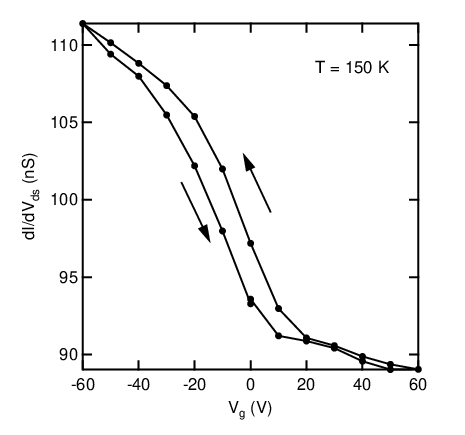
We find that the current is hysteretic with variation of . To reduce the hysteresis, we employ the following technique, in which we pulse the voltage on the gate: an AC voltage of 100 mV rms and 13 Hz is applied across the source-drain electrodes. is stepped in increments of 10 V. For each value of , the potential on the gate is applied for 5 s and the differential conductance is measured. Then is set to 0 V for 5 s to allow the sample to relax. This method reduces the hystersis because trapping of charge on a time scale greater than 5 s is eliminated. Figure 7 displays the differential conductance as a function of measured in this way at 150 K. is stepped from 0 V up to 60 V, then down to -60 V and back to 0 V. These data are consistent with those shown in Fig. 6 in that the conductance increases (decreases) as is made more negative (positive).

The temperature dependence of the current at = 6 V for different values of gate voltage is displayed in Fig. 8(a). The current is measured at a fixed temperature while the gate voltage is varied and then the current is re-plotted against inverse temperature. At each value of , the data are fit to an Arrhenius equation. As is made more negative (positive), the activation energy decreases (increases), as displayed in Fig. 8(b).
IV Discussion
The differential conductance increases (decreases) with increasing negative (positive) [Fig. 7], indicating that holes are the majority carrier in the NC solid as found previously.Talapin and Murray 2005 In bulk PbSe, unpassivated Se atoms as well as oxidation create acceptor states.Bube 1960 It is likely that the same kinds of acceptors are present in NCs, especially at the surfaces, and that these acceptor states are distributed in energy in the bandgap. The acceptors shift the Fermi energy toward the valence band of the NC solid. We believe, for reasons discussed below, that the density of states is similar to that sketched in Fig. 9(a) with the the Fermi energy lying in the acceptor states that are close to the valence band.

The temperature dependence of the zero-bias conductance [Fig. 4] is well described by an Arrhenius equation with an activation energy EA = 42 meV. We propose a model in which thermal energy is required to generate a hole in the NC from the acceptor on its surface as well as for phonon-assisted hopping between NCs with different site energies. The latter is necessary as long as the disorder in site energy is larger than the hopping matrix element between NCs. The zero bias conductivity does not distinguish between the different components of the activation energy. Rather, the activation energy is the energy between the Fermi energy and the highest-energy point in the percolation path that holes must traverse to pass from one electrode to the other. For reasons that will become apparent in the discussion of the field dependence of the conductance, it is convenient to divide the activation energy as follows: {} is the energy required to excite a hole from an acceptor state at the Fermi energy to a 1Sh state given at an energy of ;11 1 Exciting a hole from the Fermi energy to the 1Sh band is equivalent to exciting an electron from the 1Sh band to the Fermi energy. and, * is the energy required to hop between NCs, which is set by the variation in energy of the 1Sh states. This is illustrated in Fig. 10(a). Without loss of generality, we write:
| (1) |
From optical absorption of NCs in solution, we find the variation in site energy * to be 53 meV. [Fig. 2(a)]. This value is consistent with previous data of P. Liljeroth et al. who typically find that the width of the band of 1Sh states is 65 meV in an annealed film of NCs. While there are several possible contributions to the variation in site energy of NCs in a film, the similarity between * for NCs in a solution and in a film suggests that the dominant contribution is the variation in size of the NC and its consequent variation in confinement in energy. The activation energy at zero bias of 42 meV is smaller than these values, suggesting that the Fermi level lies in the tail of the 1Sh band as sketched in Fig. 9(a).

As shown in Fig. 6, the dependence of the current on source-drain voltage is essentially independent of gate voltage. This observation allows us to analyze the influence of the gate and of the source-drain voltage separately. For a given change in gate voltage, the change in the occupancy of states and the associated change in the charge density owing to the gate is in steady state. The application of results in only a small variation in the steady-state charge density because is small compared to in our measurements. Following we analyze the effect of on the activation energy and then the effect of .
As noted in connection with Fig. 5, the temperature dependence of the conductance changes with applied field. We expect the field to modify the energy required to generate a carrier: {}{} where e is the electron charge, F is the electric field and x is the distance separating an acceptor state on the surface of the NC from the 1Sh state in the core of the NC.22 2 Because of the random orientation of the NCs and the acceptors relative to the field, ionization will be faciliated by the field for only some of the acceptors. However, these are the ones which will dominate the transport at high field. The field also reduces the energy required to hop between NCs with different site energies: where d is the center-to-center distance between NCs. Thus, in the presence of a field, the activation energy is given by
| (2) |
At low fields, the slope of the activation energy versus field is . Above a critical field , given by *, charge carriers always hop to NCs with lower site energies. Thus holes always hop to NCs with higher site energies as illustrated in Fig. 10(b). Hopping no longer requires the absorption of a phonon and the slope of the activation energy versus field is simply . These two length scales are apparent in Fig. 5(b). At the highest fields (3104 V/cm F 105 V/cm), we find x = 1.10.1 nm. This is a measure of the distance between an acceptor state on the surface of the NC and the 1Sh state in the core, and is a reasonable estimate of the distance between the surface of the NC and its core. In the low field region (102 V/cm F 104 V/cm), we find x+d = 124 nm. Using the value x = 1.1 nm, we find d= 114 nm, which is within errors of 7.2 nm, the value we expect based on the size of the NCs and the thickness of the organic capping layer. The change in the slope at V/cm indicates that this is approximately the critical field. At this field the activation energy has been reduced by 20 meV, about half the variation in energy measured optically, which seems reasonable. At a sufficiently high field, tunneling between nanocrystals is expected to be limited by the height and width of the potential barrier caused by the molecules of the cap layer. However, at the highest fields used in our measurements, the current appears (Fig. 5(b)) to still be limited by thermal release of holes from the acceptor states.
The I- characteristic in Fig. 3 is consistent with this model. The conductance is ohmic at low fields (for T40 K) and becomes non-ohmic at higher fields. The crossover from ohmic to non-ohmic behavior is expected to occur when the field reduces the activation energy by an amount T. The triangles in Fig. 3 indicate the value of for which the crossover is predicted, namely where ; and, is in good agreement with the data.
Figure 8 shows how the temperature dependence of the conductance changes with gate voltage at high . As shown above, at high fields the activation energy is given by the energy required to release holes from acceptors, rather than by the energy necessary to hop between NCs. Thus the variation in the activation energy in this regime results from a shift in the Fermi energy caused by the addition of charge to the NC solid. Figure 9(a) shows the position of the Fermi energy before is applied. With the application of a negative , which removes electrons or adds holes, the Fermi energy shifts deeper into the band as illustrated in 9(b). As the voltage on the gate is made more negative (positive), decreases (increases) and the activation energy decreases (increases) as shown in Fig. 8(b). The charge density added to the film by the gate is
| (3) |
where C is the capacitance per unit area between the gate and the film, s is the screening length in the NC solid, e is the electron charge and is the density of states at the Fermi energy. The screening length can be estimated using the Thomas-Fermi expression
| (4) |
where is the dielectric constant of the NC solid. To solve for s from these two equations, we take = 250 and use the slope of the line between successive data points in Fig. 8(b) for . We find nm, approximately the size of one NC. We conclude that all the charge is added to the first monolayer of NCs adjacent to the oxide. Previous work shows that for PbSe NCs,Ben-Porat et al. 2004 but a smaller value of would only make s even smaller. This indicates that the change in conductance as a function of gate voltage [Fig. 7] results from a change in the charge density in the first monolayer only, while the conductance in the rest of the sample remains unchanged.
Knowing this, we can extract the density of states at the Fermi energy. For -20 V Vg 0 V [Fig. 8(b)], we find eV cm3 at = 6 V. An estimate of the density of the 1Sh states based on the linewidth of the optical absorption peak, the spatial density of the NCs and the 8-fold degeneracy of the 1Sh stateNimtz and Schlicht 1983; Kang and Wise 1997; Murray et al. 2001; Shcaller et al. 2003 is / eV cm3, in good agreement with the density of states derived from the data in Fig. 8(b). As Vg is made more negative than -20 V, the Fermi energy moves further into the 1Sh band and the density of states at the Fermi energy increases as reflected in Fig. 9(b). Owing to the higher density of states at the Fermi energy, more holes need to be added to the film to move the Fermi energy by a given amount. Thus a given decrease in gate voltage results in a smaller change in the Fermi energy as reflected in the decreasing slope of EA versus Vg in Fig. 8(b).
From our field effect data [Fig. 7], we extract a field-effect hole mobility in the regime where current varies linearly with . We find 4 10-5 cm2/ V s at 150 K in the regime of zero bias. Previous studies report a hole mobility of cm2/ V s from photocurrent measurements in arrays of CdTe NCs Porter et al. 2006 and a field-effect hole mobility in chemically-treated PbSe NCs of 0.09 cm2/ V s at 120 K.Talapin and Murray 2005 We find a smaller mobility most likely because our NC solids have a thicker capping layer.
Of course, our mobility is also reduced because holes are added to the NC solid at the energy of the acceptor states, not at the transport energy. However, we estimate that this reduces the mobility by no more than a factor of 10 at 150 K [Fig. 7]. One might suggest that the field-effect mobility is reduced by trapping in the oxide or at the oxide/NC-solid interface. The hysteresis that we observe in field-effect measurments indicates that there is a large enough density of slow traps to reduce the charge added to the NC solid. While the pulsed-gate technique eliminates trapping that occurs on a long time scale, it would not be surprising if there were also a large density of fast traps. However, the good agreement we find above between the experimentally derived and the expected density of states suggests that most of the charge is added to the NC solid.
The model we propose ignores Coulomb interactions between holes. On the one hand, the amount of charge added to the NC solid corresponds to of order one hole per NC in the first monolayer, and correlations are expected to be significant at these charge densities. On the other hand, the large dielectric constant of PbSe NC solids reduces the Coulomb interaction, making it likely that disorder dominates. Were many-body interactions strongly affecting the transport, we would expect the dependence of the current on field to change with gate voltage. Figure 6 shows that there is little such change.
An alternative explanation for the small activation energy seen in the zero bias conductance is that it arises from variable-range hopping (VRH) as has been speculated.Romero and Drndić 2005; Talapin and Murray 2005; Wehrenberg et al. 2005 The temperature range of Fig. 4 is not large enough to distinguish unambiguously simply activated conduction from VRH without a Coulomb gap. However, analysis of the data shows that if VRH is the dominant mechanism, then the hopping distance in the temperature range of our experiments is comparable to the distance between NCs. This would make the model no different from that of nearest-neighbor hopping, which we assume above. It is also difficult to understand how others find VRH with a Coulomb gap above 4 K.Romero and Drndić 2005; Wehrenberg et al. 2005 The high dielectric constant found in PbSe NCsBen-Porat et al. 2004 indicates that a Coulomb gap would become apparent only well below 4 K.
V Conclusions
By measuring the dependence of current on source-drain voltage, gate voltage and temperature, we have shown that our PbSe NC solids are well described by a simple model of hopping between the highest energy filled states of the NCs. After annealing, the Fermi energy is close to the edge of the highest-occupied valence level, as evinced by the small activation energy of the current and by field-effect measurements, which give a density of states close to that expected for the 1Sh band.
The activation energy is given by the energy to excite holes from acceptor states and activation over additional barriers resulting from the site disorder. By applying high electric fields, we separate these two components and measure the length scales associated with them. Not surprisingly, we find that the separation of a hole from an acceptor state occurs over a distance comparable to the spacing between the surface of the NC and its core, and the length scale associated with motion through the NC array is the center-to-center distance between NCs. Furthermore, the energy dispersion that limits the hole motion once it is free is about the same size as the energy dispersion measured by optical spectroscopy of NCs in a colloidal suspension. The density of states extracted from field-effect data is consistent with this as well. All of this suggests that the variation in energies of the localized intrinsic states is largely determined by the small variation in size of the NCs.
Acknowlegement
We are grateful to S. Amasha, I. Gelfand and I. Radu for experimental help and to S. Speakman for assistance with GISAXS. This work was funded in part by the NSF MRSEC program (DMR 0213282) at MIT and the authors made use of its shared user facilities. It was also supported by the NSEC Program of the National Science Foundation Award No. DMR-0117795 and the U.S. Army Research Office through the Institute for Soldier Nanotechnologies, under Contract No. DAAD-19-02-0002. T.S.M. gratefully acknowledges support from NDSEG.
References
- Murray et al. (1995) C. B. Murray, C. R. Kagan, and M. G. Bawendi, Science 270, 1335 (1995).
- Collier et al. (1998) C. P. Collier, T. Vossmeyer, and J. R. Heath, Annu. Rev. Phys. Chem. 49, 371 (1998).
- Markovitch et al. (1999) G. Markovitch, C. P. Collier, S. E. Henrichs, F. Remacle, R. D. Levine, and J. R. Heath, Acc. Chem. Res. 32, 415 (1999).
- Murray et al. (2001) C. B. Murray, S. Sun, W. Gaschler, H. Doyle, T. A. Betley, and C. R. Kagan, IBM. J. Res. Dev. 45, 47 (2001).
- Redl et al. (2003) F. X. Redl, K.-S. Cho, C. B. Murray, and S. O’Brien, Nature 423, 968 (2003).
- Shevchenko et al. (2006) E. V. Shevchenko, D. V. Talapin, N. A. Kotov, S. O’Brien, and C. B. Murray, Nature 439, 55 (2006).
- Whan et al. (1996) C. B. Whan, J. White, and T. P. Orlando, Appl. Phys. Lett. 68, 2996 (1996).
- Talapin and Murray (2005) D. V. Talapin and C. B. Murray, Science 310, 86 (2005).
- Novikov et al. (2005) D. S. Novikov, B. Kozinsky, and L. S. Levitov, Phys. Rev. B 72, 235331 (2005).
- Morgan et al. (2002) N. Y. Morgan, C. A. Leatherdale, M. Drndić, M. V. Jarosz, M. A. Kastner, and M. G. Bawendi, Phys. Rev. B 66, 075339 (2002).
- Drndić et al. (2002) M. Drndić, M. V. Jarosz, N. Y. Morgan, M. A. Kastner, and M. G. Bawendi, J. Appl. Phys. 92, 7498 (2002).
- Ginger and Greenham (2000) D. S. Ginger and N. C. Greenham, J. Appl. Phys. 87, 1361 (2000).
- Fischbein and Drndić (2005) M. D. Fischbein and M. Drndić, Appl. Phys. Lett. 86, 193106 (2005).
- Drndić et al. (2003) M. Drndić, R. Markov, M. V. Jarosz, M. G. Bawendi, and M. A. Kastner, Appl. Phys. Lett. 83, 4008 (2003).
- Leatherdale et al. (2000) C. A. Leatherdale, C. R. Kagan, N. Y. Morgan, S. A. Empedocles, M. A. Kastner, and M. G. Bawendi, Phys. Rev. B 62, 2669 (2000).
- Allan and Delerue (2004) G. Allan and C. Delerue, Phys. Rev. B 70, 245321 (2004).
- Wehrenberg et al. (2002) B. L. Wehrenberg, C. Wang, and P. Guyot-Sionnest, J. Phys. Chem. B. 106, 10634 (2002).
- Schaller and Klimov (2004) R. D. Schaller and V. I. Klimov, Phys. Rev. Lett. 92, 186601 (2004).
- Coe et al. (2002) S. Coe, W.-K. Woo, M. G. Bawendi, and V. Bulovic, Nature 420, 800 (2002).
- Huynh et al. (2002) W. U. Huynh, J. J. Dittmer, and A. P. Alivisatos, Science 295, 2425 (2002).
- Konstantatos et al. (2006) G. Konstantatos, I. Howard, A. Fischer, S. Hoogland, J. Clifford, E. Klem, L. Levina, and E. H. Sargent, Nature 442, 180 (2006).
- Romero and Drndić (2005) H. E. Romero and M. Drndić, Phys. Rev. Lett. 95, 156801 (2005).
- Wehrenberg et al. (2005) B. L. Wehrenberg, D. Yu, J. Ma, and P. Guyot-Sionnest, J. Phys. Chem. B 109, 20192 (2005).
- Wehrenberg and Guyot-Sionnest (2003) B. L. Wehrenberg and P. Guyot-Sionnest, J. Am. Chem. Soc. 125, 7806 (2003).
- Chen et al. (2002) F. Chen, K. L. Stokes, W. Zhou, J. Fang, and C. B. Murray, Mat. Res. Soc. Symp. Proc. 691, G.10.2.1 (2002).
- Steckel et al. (2003) J. S. Steckel, S. Coe-Sullivan, V. Bulović, and M. G. Bawendi, Adv. Mater. 15, 1862 (2003).
- Porter et al. (2006) V. J. Porter, T. Mentzel, S. Charpentier, M. A. Kastner, and M. G. Bawendi, Phys. Rev. B 73, 155303 (2006).
- Kang and Wise (1997) I. Kang and F. W. Wise, J. Opt. Soc. Am. B 14, 1632 (1997).
- Du et al. (2002) H. Du, C. Chen, R. Krishnan, T. Krauss, J. M. Harbold, F. W. Wise, M. G. Thomas, and J. Silcox, Nano Letters 2, 1321 (2002).
- Porter et al. (2007) V. J. Porter, S. Geyer, J. E. Halpert, T. S. Mentzel, M. A. Kastner, and M. G. Bawendi (2007), unpublished.
- Bube (1960) R. Bube, Photoconductivity of Solids (Wiley, 1960).
- Liljeroth et al. (2006) P. Liljeroth, K. Overgaag, A. Urbieta, B. Grandidier, S. G. Hickey, and D. Vanmaekelbergh, Phys. Rev. Lett. 97, 096803 (2006).
- Ben-Porat et al. (2004) C. H. Ben-Porat, O. Chernyavskaya, L. Brus, K.-S. Cho, and C. B. Murray, J. Phys. Chem. B 108, 7814 (2004).
- Nimtz and Schlicht (1983) G. Nimtz and B. Schlicht, in Narrow-Gap Semiconductors, edited by G. Höhler (Springer-Verlag, 1983), pp. 1–117.
- Shcaller et al. (2003) R. Shcaller, M. A. Petruska, and V. I. Klimov, J. Phys. Chem. B 107, 13765 (2003).