Defect-Tolerant CMOL Cell Assignment via Satisfiability
Abstract
We present a CAD framework for CMOL, a hybrid CMOS/ molecular circuit architecture. Our framework first transforms any logically synthesized circuit based on AND/OR/NOT gates to a NOR gate circuit, and then maps the NOR gates to CMOL. We encode the CMOL cell assignment problem as boolean conditions. The boolean constraint is satisfiable if and only if there is a way to map all the NOR gates to the CMOL cells. We further investigate various types of static defects for the CMOL architecture, and propose a reconfiguration technique that can deal with these defects through our CAD framework. This is the first automated framework for CMOL cell assignment, and the first to model several different CMOL static defects. Empirical results show that our approach is efficient and scalable.
1 Introduction
In recent years, nanoelectronics has made tremendous progress, with advances in novel nanodevices [18], nano-circuits [1, 5], nano-crossbar arrays [2, 8, 12], manufacture by nanoimprint lithography [19, 10], CMOS/nano co-design architectures [9, 3, 20], and applications [16, 15, 17]. Although a two-terminal nanowire crossbar array does not have the functionality of FET-based circuits, it has the potential for incredible density and low fabrication costs [9]. Likharev and his colleagues [9] have developed the concept of CMOL (Cmos / nanowire / MOLecular hybrid) as a likely implementation technology for charge-based nanoelectronics devices. Examples include memory, FPGA, and neuromorphic CrossNets [16, 15, 17].
In this paper, we present a framework for CMOL cell assignment. We transform any boolean circuit based on AND/OR/NOT gates to a circuit of NOR gates, and then map the NOR gates to the CMOL architecture. We formulate the CMOL cell mapping task as a set of boolean conditions, and solve them through satisfiability. Prior work on CMOL [9] was assigning cells by hand. Our technique is the first automated CMOL cell assignment framework. We further investigate various defect models for the CMOL technology, and propose a reconfiguration technique that can deal with all these defects through our cell assignment framework. This is the first detailed study on numerous CMOL defect models.
2 Background about CMOL

CMOL was originally developed by Likharev and his colleagues [9]. The nanodevice in CMOL is a binary “latching switch” based on molecules with two metastable internal states. Fig. 1 shows the schematic I-V curve of this two-terminal nanodevice. Qualitatively, if the drain-to-source voltage is low during programming, the nanodevice will be in the “off” state with a high resistance; if the applied voltage is greater than a certian value, the nanodevice will be in the “on” state with a lower resistance. In the operating mode, if the nanodevice is in the “on” state and the applied voltage to the drain and source is greater than the threshold voltage , the I-V curve will be like the I-V curve of a finite resistor. If the applied voltage is less than threshold voltage, then the nanodevice is virtually in the “off” state. However, it is not certain yet how large the on-off resistances are and how long the nanodevice can keep its programmed state. From our previous analysis [6], for an aggressive assumption of CMOL’s parameters with 6 nm nanowire pitch, the nanodevice “on” resistance could exhibit a higher value than that of a reasonable length of nanowire (e.g., 6 m). To avoid routing the critical signal path via multiple nanodevices is one of the synthesis and routing rules we need to be aware of. In this paper, we address the CMOL cell assignment problem with the understanding that routing between two cells through the nanowire fabric will involve one nanodevice only (see Section 3.2).
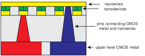
Fig. 2 shows the basic CMOL circuit, especially the interface between CMOS and nanowires. The pins connect the CMOS upper-level metals and the nanowires. The nanodevices are sandwiched between the two levels of perpendicular nano-imprinted nanowires. This unique structure solves the problems of addressing much denser nanodevices with sparser CMOS components. Each nanodevice is accessed by the two perpendicular nanowires which connect to the nanodevice. The nanowires are in turn connected by the pins which interface with the CMOS circuits. With nanowires and pins, we could address nanodevices.
Strukov and Likharev [15, 14] proposed the CMOL FPGA idea to fully explore the regularity of the CMOL architecture. Because the nanodevices are non-volatile switches, the CMOL FPGA could program those nanodevices and route the signals from CMOS to the nanowires and nanodevices, and back to CMOS again. All logic functions should be done in the CMOS level. To further explore the architectural regularity, they proposed cell-like CMOS stucture, as shown in Fig. 3. In each cell, there is an inverter in the CMOS level. One direction of nanowires receive signals from the outputs of the inverters in the CMOS level. Those nanowires are OR’ed together with another direction of nanowire according to the nanodevice configurations in the nanowire level. The OR’ed signal goes to the inverter’s input, which is on the CMOS level. This OR-NOT logic is the fundamental logic of CMOL FPGA. Any combinational logics should be expressed in the OR-NOT (or NOR) way. For example, in Fig. 3, are three signals connected with the three grayed cells’ output pins. With the illustrated nanowire connections (brown lines) and “ON” nanodevices (green dots), the logic expression is .

Based on Strukov and Likharev’s CMOL FPGA, Snider and Williams [11] proposed field-programmable nanowire interconnect (FPNI) with more conservative circuit parameters than CMOL FPGA’s, such as wider nanowires and wider nanowire pitches, sparser crossbar arrays, and larger pins. Moreover, the FPNI assumes combination of logic gates (e.g., NAND/AND), buffers, flipflops in the CMOS cell (or hypercell), which is similar to the concurrent CMOS FPGA architectures. Although the area consumption of the FPNI is larger than that of the CMOL FPGA, it shows at least one order of magnitude of reduction in area compared with CMOS FPGA [11]. And FPNI should be much more practical for manufacturing than CMOL FPGA as projected in 10 years [11].
Strukov and Likharev [15] presented the CMOL FPGA and performed cell assignment task manually for simple regular-structured boolean circuits. They also presented a reconfigurable architecture [14] for CMOL FPGA, that grouped CMOL cells to form lookup-tables (LUTs), which can utilize existing (LUT-based) FPGA CAD tools.. However, that work also did not solve the CMOL cell assignment problem. In this paper, we solve the CMOL cell assignment problem via satisfiability and extend it as a reconfiguration tool for various CMOL defects.
3 CAD Framework
The CMOL architecture presented by [15] is capable of implementing a circuit of NOR gates, as explained in Fig. 3. This means the logic synthesis front-end must present a circuit in terms of NOR gates. We can then place and route these NOR gates on the CMOL cells. There are many logic synthesis tools that can optimize boolean circuits based on AND/OR/NOT gates, but there are not much recent work on optimization of NOR gate circuits. In this section, we first present a simple algorithm to convert any circuit of AND/OR/NOT gates into a circuit of NOR gates. We then describe how to do routing on CMOL cells and present our satisfiability-based cell assignment method. We use an adder as an example to illustrate our ideas.
3.1 NOR Gate Transformation
Given any boolean circuit in terms of AND/OR/NOT gates, we want to transform the AND gates and OR gates into NOR gates (NOT gates are considered as single input NOR gates). The pseudo code is shown in Algorithm 1. We use De Morgan’s law to convert AND/OR to NOR gate (lines 3 and 5), also shown in figure 4. We then remove stacked inverters in lines 8–14. We use to denote the set of gates that drive the input of gate . The double for loop from line 15 to line 22 will remove duplicated inverters. Notice that the complexity of this double for loop can be reduced if we hash all the gates based on inputs nets (i.e., performance speedup).

Theorem 1
For any boolean circuit in the Product-of-Sum (POS) format with at least one AND gate and all its inputs driven by OR gates, Algorithm 1 will result in a NOR gate circuit with the same number of NOR gates as the number of (AND/OR/NOT) gates in the original POS circuit.
Proof: The AND gate will be converted into a NOR gate with inverters at its input. Similarly, the OR gates will be converted into NOR gates with inverters at the output. Since all OR gate outputs are connected to the AND gate and all AND gate inputs are driven by OR gates, we will end up with inverters driving inverters which can be easily eliminated. Hence the number of gates remains the same.
3.2 Routing
Routing between CMOL cells is pre-determined by the nanowire fabric. Each CMOL cell has one output nanowire and one input nanowire which are orthogonal to each other. The input nanowires for all CMOL cells are oriented in the same direction (parallel), and the same property is true for all the output nanowires. Hence, there is only one intersection between the output nanowire of one CMOL cell and the input nanowire of another CMOL cell. If we want to connect these two cells, we need to program the nanodevice at the corresponding intersection to be “ON”. For example, in figure 3, the output nanowire of cell and the input nanowire of cell has a unique intersection shown on the left side of the figure. By turning the corresponding nanodevice ON or OFF, we can connect or disconnect the route from to respectively.
According to [15], there are periodic breaks in the nanowire fabric, such that each input/output nanowire has a fixed length based on the period. Hence each CMOL cell can only be connected to a limited number of neighboring CMOL cells. The set of CMOL cells that can be connected to the input of a particular cell is called the input connectivity domain of . Similarly, the output connectivity domain refers to the set of cells that can be connected to the output of .
Although the input/output connections between any two CMOL cells through the nanowire fabric is pre-determined and limited by the connectivity domain, it is still possible for one cell to communicate with cells outside its connectivity domain. For example, cell send its output to cell (which is within the connectivity domain of ), and then cell can send its output to cell (which is inside the connectivity domain of but outside the connectivity domain of ). However, some physical constraints may prevent people from using this idea for timing critical paths [6]. In addition, the CMOL architecture implements the NOR logic (or NOT gate for single input case), we may have to use two intermediate cells (i.e. two inverters) to maintain the same logic polarity. This idea is similar to buffer insertion in traditional ASIC CAD flow. For the rest of this paper, we assume that these types of connecting through multiple CMOL cells is handled by the generation of logic circuit, which can be done through logic synthesis.
3.3 CMOL Cell Assignment
We are given a collection of CMOL cells, the number of cells in this collection is . Each CMOL cell is as described in Figure 1 of [15]. These CMOL cells can come in rectilinear fashion as described in Fig. 3 but our satifiability formulation does not require them to be of any regular shape.
We assume that each CMOL cell can be connected to a set of CMOL cells, where
An example for is the “connectivity domain” as described in section 3.2. Notice that the “connectivity domain” described in [15] has a regular pattern around the neighborhood of each CMOL cell . But the in our satisfiability formuation can be arbitrarily any subset of CMOL cells which does not require them to have any regular pattern. Figure 5 illustrates such non-regular-patterned connectivity domain.

We are given a NOR gate circuit , which can be produced by Algorithm 1 or other methods. We can represent the circuit as a graph where is the set of nodes and is the set of edges in the graph. The nodes corresponds to the gates in the circuit, whereas the edges corresponds to the nets (gate-to-gate connections) in the circuit, i.e., . For ease of denotation, we will refer to the gates as and the nets as respectively. Notice that if-and-only-if the output of gate is connected to the input of gate for all gates . We have:
The CMOL cell assignment problem is to place the circuit on such that each gate will occupy one-and-only-one CMOL cell, and the input-output connectivity of each NOR/NOT gate in the assigned CMOL cell falls within the “connectivity domain” . We can describe the CMOL cell assignment problem mathematically as an injective function :
where
| (1) | |||
| (2) |
We now propose a satisfiability-based (SAT) approach for solving the CMOL cell assignment problem. We first introduce a set of boolean variables to encode the various possibilities of placing NOR gates to CMOL cells. We then formulate the boolean constraints to characterize the injective nature of the mapping and the CMOL requirements.
Let be a Boolean variable that represent the assignment of gate on CMOL cell , where and .
Since each gate must be assigned to at most one CMOL cell, we have:
| (3) |
In addition, each gate must be assigned to at least one CMOL cell:
| (4) |
We cannot assign two or more gates to the same CMOL cell:
| (5) |
The connected gates in the circuit must be placed within the connectivity domain:
| (6) |
We construct a satisfiability formula by conjuncting all the above constraints (3), (4), (5), (6). We feed all the above constraints to a SAT solver. The solution that satisfies the conjunction is the cell assignment result.
We can introduce more constraints to address practical issues of the cell assignment problem. For example, our formulation so far allows any NOR gate to be assigned to any CMOL cell, as long as it fits all the above constraints. However, under certain situations, we want to prevent the assignment of a certain gate to a subset of CMOL cells. To handle such cases, we simply have to set the boolean variable to be FALSE, where . We can then propagate constants through the boolean formulations and simplify the problem.


Notice that the cell assignment method presented here is designed to address technology-specific issues for the CMOL architecture at the lowest design module level. A top-down hierarchical approach of both global placement and detailed placement techniques should be used for large designs.
Contemporary SAT solvers are architected to terminate early as soon as any solution is found. If no solution exists, the SAT solver will search all possible cases and essentially prove to us that the problem is unsolvable. Notice that if there are more than one solutions to the problem, the SAT solver tend to finish very fast. Satisfiability has been used to solve a variety of problems [13, 7]. Many commercial CAD tools in industry also use SAT solvers in their CAD flow.
3.4 Example: Adder
We first experiment with a simple full adder as an example. Figure 6(a) shows the logic structure of a full adder in product of sum format. The adder has 3 inputs (, , ) and 2 outputs (, ). Using our transformation technique in section 3.1, we converted the logic circuit to NOR format as shown in figure 6(b). We then feed the NOR circuit to our CMOL cell assignment tool, and specified a region with the following restrictions:
- •
inputs and must be located at the left 3 cells (only 2 are needed)on the top row;
- •
input must be located at the right column at the second cell from the bottom up;
- •
output must be located at the left column at the second cell from the bottom up (corresponding row with );
- •
output must be located within the left 3 cells at the bottom row; and
- •
all other gates must be located within the lower left CMOL cell region.
All these restrictions are fed to the SAT constraints by setting the corresponding cell assignment variables to be constant.
The result is shown in figure 7. For each CMOL cell, we use a red dot at the lower-left (and a blue dot at the upper-right) to indicate the output (input) terminals, respectively. The lines connecting the dots are corresponding to the interconnection between the NOR gates in figure 6(b). Notice that these lines are simple logic connection indicators, and should not be confused with the nanowire crossbar which should be regularly oriented at an angle relative to the square array of the cells.
4 Defect Tolerance
There are many possible causes of defect to the CMOL implementation as illustrated in figure 8. In the figure, we use to denote the nanowires, and to denote the nanodevices, respectively. The nanodevice (colored gray) is defective, like a pre-programmed “OFF” (stuck-open). The nanodevice (colored green) has a different defect, like a short-circuit. It is pre-programmed “ON” (stuck-closed). are non-defective (colored pink). They can be programmed “ON” or “OFF” by the user.

Given CMOL cells , , and in figure 8, and assuming there are no defects, we can implement through . If nanowire is broken (defect), we have to use CMOL cell instead of , and program “ON”. So , where replaces . If is stuck-open, then it doesn’t matter is broken or not, we cannot connect cells and . In this case, we can either use to replace like above, or we can use to replace , and enable and , such that , where replaces .
In general, we can foresee the following types of defects for the CMOL architecture:
- 1.
A (input/output) nanowire for a CMOL cell is broken into two or more segments. Hence the CMOL cell may not be able to connect to all other CMOL cells within its input/output connectivity domain or radius (where ). In this case, the CMOL cell is still useful but its connectivity domain should be modified into a different shape.
- 2.
The nanodevice connecting two perpendicular nanowires (let’s say the output nanowire of cell A and input nanowire of cell B) is stuck-at-open. In this case, the connection from A to B through this nanodevice is broken. But these two CMOL cells can still be used. We simply have to modify the connectivity domains such that A is outside the input connectivity domain of B, and B is outside the output connectivity domain of A.
- 3.
The nano-device connecting two perpendicular nanowires (let’s say the output nanowire of cell A and input nanowire of cell B) is stuck-at-closed. In this case, A will always be in the NOR gate input of B. To optimize the CMOL cell usage, we have two choices:
- •
Do not use cell B, but cell A can still be used if we desire.
- •
Assign a NOR gate in cell B, and assign one of B’s inputs to cell A.
- •
- 4.
Something else is wrong with a CMOL cell randering this cell to be usuable, including (but not limited to) the following:
- •
the input/output terminal connecting the CMOS layer and the input/output nanowire is broken
- •
the CMOS inverter is broken
- •
Notice that prior work [15] is mainly focused on our defect type 2 above. This paper is the first attempt to address various other types of defects.
We can formulate the above 4 defects using satisfiability constraints.
For defect types 1 and 2, the input/output connectivity domain for the CMOL cells related to the defect should be modified. Notice that our cell assignment formulation in section 3.3 does not assume any regularity for the connectivity domains, so it can be modified to arbitrary shape depending on the defect.
For defect type 3, the CMOL cell A will always be one of the NOR gate input for CMOL cell B. We need to make sure that any node with no fanin (i.e. primary input) cannot be assigned to cell B. This can be easily done by setting the corresponding cell assignment variables at cell B to FALSE.
| (7) |
for all where .
We also need to make sure that any gate assigned to cell B must have one of its input placed at cell A.
| (8) |
for all where .
For defect type 4, we cannot assign any gate to the defective CMOL cell. Hence we must set the cell assignment variable of every gate at that cell to FALSE.
| (9) |
for all , and is the defective CMOL cell.
Given a manufactured CMOL device with some known defects, and an initial mapping (most likely done before the manufacturing) that did not take those defects into account, we need to reconfigure the CMOL device to work around those defects. We can use the following algorithm for the reconfiguration:
Our algorithm takes advantage of the idea that many defects in the real world tend to be clustered together. So we use a center of mass computation to focus our reconfiguration region on the affected cells.
5 Experiments
Besides the adder example, we conducted experiments on ISCAS benchmarks. For each design, we first carve out the combinational logic, i.e., convert all inputs/outputs of latches (or sequential elements) to primary outputs/inputs respectively. We then run the SIS sweep operation to simplify the circuit (and remove redundant gates). We convert the circuit to NOR gates using the simple algorithm in Section 3.1. To make sure that our logic transformations are correct, we formally verified the logic correctness of the transformation results using equivalence checkers. Finally, we assign the NOR gates to CMOL cells using our method in Section 3.3. The CMOL cell region for each design was choosen to be a square shaped (or nearly square) territory where the number of cells is slightly more than the number of NOR gates in the circuit. We also put special restriction so that the primary inputs/outputs are located around the perimeter of the square region. We use the connectivity domain with radius as specified in [15]. We ran our satisfiability constraints through the MiniSAT [4] solver to generate the cell assignment. All experiments are performed on Linux with a 1.5GHz Intel Pentium 4 CPU with 3GB memory. Table 1 summarizes our experiments. The inputs/outputs column shows the primary inputs/outputs after carving out the combinational part of the benchmark design. The cells column shows the number of NOR/NOT gates that need to be assigned to CMOL cells. The X and Y dimensions show the size of the cell assignment territory. The vars and clauses indicate the size of the CNF generated for the satisfiability formulation. The time column indicates the CPU seconds that the MiniSAT took to solve the problem.
| Circuit | inputs | outputs | cells | X | Y | vars | clauses | time (sec) |
|---|---|---|---|---|---|---|---|---|
| adder | 3 | 2 | 12 | 4 | 5 | 135 | 1577 | 0.01 |
| s208 | 18 | 9 | 136 | 13 | 12 | 18246 | 2444373 | 509.84 |
| s27 | 7 | 4 | 19 | 5 | 5 | 376 | 7164 | 0.07 |
| s298 | 17 | 20 | 122 | 13 | 12 | 14962 | 1829223 | 370.30 |
| s344 | 24 | 26 | 179 | 14 | 14 | 27884 | 4595793 | 6.18 |
| s349 | 24 | 26 | 184 | 14 | 14 | 28864 | 4834296 | 7.60 |
| s382 | 24 | 27 | 175 | 14 | 14 | 26956 | 4377249 | 12.88 |
| s386 | 13 | 13 | 164 | 14 | 13 | 26416 | 4278318 | 10.30 |
| s400 | 24 | 27 | 188 | 15 | 14 | 31524 | 5540402 | 7.52 |
| s444 | 24 | 27 | 187 | 15 | 14 | 31314 | 5489242 | 7.59 |
| s510 | 25 | 13 | 266 | 18 | 18 | 88768 | 26315936 | 213.27 |
For defect tolerance, we inject the various defects mentioned in section 4 to the cell assignments in Table 1. For each design, we first pick a randomly generated location , and then compute a probability density function for each location using the Gaussian distribution.
This probability density function is used to control the injection of defects. For each defect type, we generate a random floating point number between 0 and 1 at each location where the defect can happen. The defect is injected if . The cumulative SAT solver runtime that Algorithm 2 took for each design is shown in Table 2.
| Circuit | ||
|---|---|---|
| s208 | 0.26 | 0.12 |
| s298 | 0.11 | 0.42 |
| s344 | 0.21 | 0.31 |
| s349 | 0.26 | 0.45 |
| s382 | 0.18 | 0.25 |
| s386 | 0.14 | 4.00 |
| s400 | 0.02 | 0.61 |
| s444 | 0.01 | 0.48 |
| s510 | 0.12 | 0.06 |
6 Conclusion
In this paper, we present a CAD framework for the CMOL architecture. We transform any netlist of AND/OR/NOT gates to a NOR gate circuit, and then map the NOR gates to CMOL cells. Our CMOL cell assignment is based on satisfiability and it can generate the assignment if and only if the solution exists. We also present a model for various types of defects under the CMOL architecture, most of which has never been studied before. We present a reconfiguration technique that can deal with all these defects through our CAD framework. This is the first work on automated CMOL cell assignment, and the first to model and tolerate several different CMOL defects. Our experiments indicate that our reconfiguration technique is fast and scalable.
References
- [1] A. Bachtold, P. Hadley, T. Naknishi, and C. Dekker. Logic circuits with carbon nanotube transistors. Science, 294:1317–1320, 2001.
- [2] Y. Chen, G.-Y. Jung, D. A. A. Ohlberg, X. Li, D. R. Stewart, J. O. Jeppesen, K. A. Nielsen, J. F. Stoddart, and R. S. Williams. Nanoscale molecular-switch crossbar circuits. Nanotechnology, 14:462–468, 2003.
- [3] A. DeHon and e. al. Stochastic assembly of sublithographic nanoscale interfaces. IEEE Trans. on Nanotechnology, 2:165–174, 2003.
- [4] N. Een and N. Sorensson. Translating Pseudo-Boolean Constraints into SAT. Journal on Satisfiability, Boolean Modeling and Computation, 2:1–26, 2006.
- [5] R. S. Friedman, M. C. McAlpine, D. S. Ricketts, D. Ham, and C. M. Lieber. High-speed integrated nanowire circuits. Nature, 434(28):1085, 2005.
- [6] C. Gao and D. Hammerstrom. Cortical models onto CMOL and CMOS - architectures and performance/price. submitted to IEEE Tran. on Circuits and Systems - I, 2007.
- [7] W. N. N. Hung, X. Song, E. M. Aboulhamid, A. Kennings, and A. Coppola. Segmented Channel Routability via Satisfiability. ACM Transactions on Design Automation of Electronic Systems, 9(4):517–528, October 2004.
- [8] P. J. Kuekes, D. R. Stewart, and R. S. Williams. The crossbar latch: logic value storage, restoration, and inversion in crossbar circuits. Journal of Applied Physics, 97:034301–1–5, 2005.
- [9] K. K. Likharev and D. V. Strukov. CMOL: devices, circuits, and architectures. In G. Cuniberti and et al., editors, Introduction to Molecular Electronics, pages 447–477. Springer, Berlin, 2005.
- [10] D. J. Resnick, W. J. Dauksher, D. Mancini, K. J. Nordquist, T. C. Bailey, S. Johnson, N. Stacey, J. G. Ekerdt, C. G. Willson, and S. V. Sreenivasan. Imprint lithography for integrated circuit fabrication. Journal of Vacuum Science & Technology B: Microelectronics and Nanometer Structures, 21:2624, 2003.
- [11] G. Snider and R. Williams. Nano/cmos architectures using a field-programmable nanowire interconnect. Nanotechnology, 18:1–11, 2007.
- [12] G. S. Snider, P. J. Kuekes, and R. S. Williams. CMOS-like logic in defective, nanoscale crossbars. Nanotechnology, 15:881–891, 2004.
- [13] X. Song, W. N. N. Hung, A. Mishchenko, M. Chrzanowska-Jeske, A. Coppola, and A. Kennings. Board-level multiterminal net assignment for the partial cross-bar architecture. IEEE Transactions on VLSI Systems, 11(3):511–514, June 2003.
- [14] D. Strukov and K. Likharev. A reconfigurable architecture for hybrid CMOS/nanodevice circuits. In FPGA’06, pages 131–140, Monterey, California, USA, 2006.
- [15] D. B. Strukov and K. K. Likharev. CMOL FPGA: a reconfigurable architecture for hybrid digital circuits with two-terminal nanodevices. Nanotechnology, 16(6):888–900, 2005.
- [16] D. B. Strukov and K. K. Likharev. Prospects for terabit-scale nanoelectronic memories. Nanotechnology, 16:137–148, 2005.
- [17] O. Türel, J. H. Lee, X. Ma, and K. K. Likharev. Architectures for nanoelectronic implementation of artificial neural networks: new results. Neurocomputing, 64:271–283, 2005.
- [18] J. Xiang, W. Lu, Y. Hu, Y. Wu, H. Yan, and C. M. Lieber. Ge/Si nanowire heterostructures as high-performance field-effect transistors. Nature, 441(25):489–493, 2006.
- [19] S. Zankovych, T. Hoffmann, J. Seekamp, J.-U. Bruch, and C. M. S. Torres. Nanoimprint lithography: challenges and prospects. Nanotechnology, 12:91–95, 2001.
- [20] M. M. Ziegler and M. R. Stan. CMOS/nano co-design for crossbar-based molecualr electronic systems. IEEE Transactions on Nanotechnology, 2(4):217–230, 2003.