Conflict of interest footnote placeholder
This paper was submitted directly to the PNAS office.
Abbreviations: 2D, two dimensional; MOSFET, metal oxide semiconductor field effect transistor; RPA, random phase approximation
Submitted to Proceedings of the National Academy of Sciences of the United States of America
A self-consistent theory for graphene transport
Abstract
We demonstrate theoretically that most of the observed transport properties of graphene sheets at zero magnetic field can be explained by scattering from charged impurities. We find that, contrary to common perception, these properties are not universal but depend on the concentration of charged impurities . For dirty samples (), the value of the minimum conductivity at low carrier density is indeed in agreement with early experiments, with weak dependence on impurity concentration. For cleaner samples, we predict that the minimum conductivity depends strongly on , increasing to for . A clear strategy to improve graphene mobility is to eliminate charged impurities or use a substrate with a larger dielectric constant.
keywords
graphene — electron transport — minimum conductivityT he past two years have seen a proliferation of theoretical and experimental interest in graphene. The interest stems mainly from the striking differences between graphene and other more well known semiconductor-based two dimensional (2D) systems, that arise mostly from its unique band structure, obtained by considering graphene to be a single sheet of carbon atoms arranged in a honey-comb lattice. Graphene is in fact a carbon nanotube rolled out into a single 2D sheet, and as was already known from studying carbon nanotubes, electrons moving in the periodic potential generated by the carbon lattice form a band that displays striking properties such as having a chiral Dirac equation of motion with a mathematical structure similar to Weyl neutrinos. This intriguing ‘relativistic’ Dirac-Weyl spectrum of graphene has attracted substantial interest and attention. While this analogy of considering graphene as a solid-state realization of the “massless chiral Dirac Fermion” model (developed as a solution to Dirac’s Lorentz invariant generalization of Schrödinger’s equation) has some utility, it also has the potential to be misleading. In particular, as we argue here, searching to explain the experimental transport properties of graphene by focusing on the “Dirac point” (see formal definition below), obscures the real mechanism of carrier transport. In this respect, and from our perspective, the physics of graphene has more in common with the Metal-Oxide-Semiconductor-Field-Effect-Transistors (MOSFETs) that form the backbone of our current day semiconductor industry, than with the physics of relativistic chiral Fermions. Studying graphene is therefore as much about making useful MOSFETs from pencil smudges, as it is about studying quantum electrodynamics in a pencil mark.
We observe that already within one year since the fabrication of the first gated 2D graphene samples (that enable a variable external gate voltage tuned carrier density), mobilities as high as have been reported, and these values are comparable to the best Si MOSFET samples at low temperature. In addition, graphene mobility is relatively temperature independent, making room temperature 2D graphene mobilities to be among the highest in FET type devices. It is therefore both of fundamental and technological interest to understand the transport mechanism in graphene in reasonable qualitative and quantitative detail. Similar to MOSFETs, transport properties of graphene are determined by scattering from charged impurities which are invariably present. We report here the essential graphene transport theory focusing on charged impurity scattering.
Prior to this work, the conventional wisdom in the graphene community was that close to the Dirac point, carrier transport is ballistic, that the minimum conductivity is universal and that we lack a basic understanding of how at the Dirac point there could be carrier free transport over micron-sized distances. In this context, our work provides a theoretically simple explanation for this graphene transport mystery: charged impurities in the substrate generate carrier density fluctuations that allow for non-universal diffusive transport, and that these density inhomogeneities render the Dirac point physics experimentally inaccessible, at least for current graphene samples (see note added at the end of this paper).
We emphasize that although the importance of charged impurity scattering in determining the linear-in-density high-density (i.e. far from the charge neutral Dirac point) graphene carrier transport has already been established [1, 2, 3, 4] in the literature, the current work is the first to point out that the same charged impurities will have a qualitative effect at low carrier density close to the Dirac point by providing an inhomogeneous electron-hole puddle landscape where the conductivity will be approximately a constant over a finite range of external gate voltage, providing a simple and physically appealing explanation for the observed graphene minimum conductivity plateau. The importance of our work therefore lies in its ability to explain the graphene transport data at low carrier density through a physically appealing charged impurity-induced mechanism which quantitatively explains both the existence (and the width) of the minimum conductivity plateau as well as its magnitude. No such explanation existed in the literature before our work, and the minimum conductivity phenomenon in graphene was considered to be an outstanding experimental puzzle.

In this context, “bare graphene” is the empty honeycomb lattice, where allowing for electron hoping between adjacent sites gives the linear Dirac-Weyl spectrum. The nominally undoped or ungated situation is that of the completely filled valence band and a completely empty conduction band which touch at the Dirac point making graphene a zero-gap semiconductor. The Dirac point is a singular point of measure zero that separates the conduction and the valence band in the linear graphene spectrum. This “intrinsic graphene” with the chemical potential (or Fermi energy) precisely at the Dirac point has no free carriers and is obviously an abstract model, since the slightest amount of doping or external potential will induce carriers in the system. Charged impurity disorder or spatial inhomogeneity will render this intrinsic graphene experimentally unrealizable. “Extrinsic graphene” is when one induces free carriers (either electrons in the conduction band with a positive potential, or holes in the valence band with a negative potential), by applying an external gate voltage , or equivalently, by doping the system. Carrier bands are filled up to a certain Fermi Energy , determined by the electrostatic potential configuration of the graphene environment, and depending on which is larger, could be dominated either by the external gate voltage or by charged impurities. All experimental graphene samples are extrinsic, since there are invariably some free carriers present in the system, and transport close to the Dirac point is dominated by two distinct effects of the charged impurities in the system: (i) the induced graphene carrier density is self-consistently determined by the screened charged impurity potential; and (ii) the conductivity is determined by charged impurity scattering.
As one would expect with any newly discovered electronic material [7], the full gamut of experimental techniques has been used to explore graphene properties, including light scattering [8], angle resolved photo-emission spectroscopy [9], and surface probe measurements [10, 11]. The field continues to evolve with new ideas being explored including making suspended graphene [12] and electromechanical resonators [13], transfer-printing graphene onto plastic [14], using superconducting [15] and ferromagnetic leads [16], having patterned top-gates [17, 18, 19], exposing samples to molecular dopants [20] and fabrication of graphene-nano-ribbons [21]. These rapid experimental advances show that the study of graphene is still in its infancy, with many promises for the discovery of new physics and for application to technology.
The focus of the present work is on the important graphene transport measurements [6, 22]. These were the first experiments to be done, and are still not understood, in that there are widely disparate claims on the transport mechanism. Since these experiments form the basis for most of the future work on graphene as well as its prospective technological applications, a correct understanding of the basic transport physics is of fundamental importance. While there are many features observed in the transport experiments, two have been highlighted and particularly discussed in the literature, namely, the low-density “minimum conductivity” , i.e. the value of the conductivity at or near the Dirac point (where , and a naïve picture would suggest that there are no charge carriers); and the high-density conductivity which is linear in the carrier density , giving a constant mobility . As we discuss below, our analytic theory is the first to explain both features quantitatively, as well as make predictions for the width of the minimum conductivity plateau and the offset of the Dirac point from zero gate voltage.
In the literature, most theoretical work has focused on the short-range scattering mechanism (also called “white noise” disorder) to understand graphene transport, mainly as a matter of technical convenience. Early work using a Kubo formalism in the ballistic limit [23, 24] showed that the conductivity for massless Dirac Fermions is for vanishing disorder, and that this universal value occurs only at the Dirac point and not in its vicinity. At finite carrier density, the Kubo formalism with short-range scattering gives a conductivity that is constant with carrier density [1] and not the linear in density behavior seen in experiments. Certain numerical [2] and analytical [25] methods that try to extrapolate between these two limits inevitably get a square-root dependence of conductivity on density (not linear), and give orders-of-magnitude incorrect values for the mobility. More recently, short range scattering has been considered theoretically [26, 27, 28] with the finding that at zero temperature, localization effects should give . While all these works improve our abstract theoretical understanding of graphene, they are all in qualitative disagreement with existing experimental data. We argue here that short-range scattering has little to do with the experiments of Refs. [7, 6, 22], and that although localization effects may very well be important in the zero temperature limit, the existing bulk graphene transport data at accessible temperatures () are in the Drude-Boltzmann diffusive transport regime. Equally important, the observed transport properties of doped graphene do not access the Dirac point physics, at least in the currently available samples [6, 22] which have fairly large concentrations of charged impurity centers. While the observed conductivity value (and not conductance) of in dirty samples brings to mind connections with universal conductance quantization phenomena such as one-dimensional point-contact conductance quantization or Zitterbewegung or quantized Hall resistance, we argue here that no such universal physics is at play in current bulk graphene transport experiments where conductivity, and not conductance is being discussed.
Our goal here is to develop a quantitatively accurate analytic theory for the most important graphene transport problem, namely, the regular bulk dc conductivity studied in the diffusive Drude-Boltzmann limit, which is the regime of technological interest. We argue that charged impurity scattering is responsible for most of the observed bulk diffusive transport behavior in graphene. Charged impurities could reside either inside the substrate or created near the graphene-substrate interface during the processing and handling of samples. The typical concentration of charged impurities in a SiO2 substrate is , and are known to dominate the transport properties of other extensively studied 2D semiconductor systems [29].
Earlier work [2, 3, 4] demonstrated that while the mean free path for short-range scatterers , where is the carrier density, for Coulomb (i.e. charged impurity) scatterers . This implies that although graphene at low density is a clean or ballistic system for short-range scatterers, it is a dirty and diffusive system for long-range scatterers. At low carrier densities of , one can estimate that and . Therefore, at the lowest densities close to the Dirac point, graphene transport properties are completely dominated by Coulomb scattering. This simple argument also establishes that any short-range scattering, even if it is present in graphene, is irrelevant in the low carrier density limit near the Dirac point where the minimum conductivity plateau is observed.
In the present work we provide a complete picture of transport in both high and low carrier density regimes using a self-consistent RPA-Boltzmann formalism where the impurity scattering by the charged carriers themselves is treated self-consistently in the Random Phase Approximation (RPA), and the dc conductivity is calculated in the Boltzmann kinetic theory. We derive analytic expressions for (i) mobility , (ii) plateau width, (iii) minimum conductivity, and (iv) shift in gate voltage. Our results for graphene on a SiO2 substrate can be summarized as
where Eq. A self-consistent theory for graphene transport below gives analytic expressions for and .
An important finding of our work is that for dirty samples with , is indeed close to as observed experimentally, and not very sensitive to changes in disorder, while for cleaner samples with , , and is sensitive to the value of , thus explaining the mystery of why more recent experiments show a larger magnitude and larger spread in the value of . For the typical densities used in the early graphene experiments, the minimum conductivity appears to saturate at a universal value of , but we predict that there is nothing universal here, and for dirtier samples, the value of the minimum conductivity as a function of would slowly decrease.
The formalism developed here to obtain Eq. A self-consistent theory for graphene transport can be divided into three steps. First, we develop an analytical solution for the Boltzmann transport theory using the full RPA treatment of the charged impurity scattering. We find analytically that in agreement with earlier numerical calculations [2, 3, 4]. Second, we extend the methods of Refs. [5, 30] to evaluate the screened voltage fluctuations induced by charged impurities. Here we calculate the potential fluctuations using the full RPA screening, which although being complicated and cumbersome, is necessary to obtain quantitative agreement. Third, we develop a theory to calculate the residual carrier density self-consistently. We find that the ratio , that is directly related to the minimum conductivity through , is a monotonically decreasing function of and the dependence gets weaker for larger impurity density.
Before we provide details of our calculation, we first address the range of validity of our self-consistent RPA-Boltzmann theory. First, we consider only Coulomb scattering. As already discussed above (see also Ref. [4]), other scattering mechanisms are irrelevant at low density and the experimentally observed linear dependence of conductivity with carrier density singles out charged impurities as the dominant scattering mechanism. Only in the limit of very small charged impurity density, must one include short-range scattering into the formalism (such short-range scattering may arise from point-defects and dislocations in the lattice). We find , where we estimate , suggesting that for very low impurity densities (two orders of magnitude lower than present day samples), will saturate at around , before our charged impurity model gives way to short-range scattering. Second, our theoretical calculation is done at zero temperature. Theoretically one expects [3] very weak temperature dependence for , and this is indeed consistent with experimental observations where . Third, since the sample sizes are several microns in length, and the mean free path is tens of nanometers, we are certainly in the diffusive as opposed to ballistic transport regime. Fourth, electron interactions are treated within the RPA approximation scheme. RPA is an expansion in , and in graphene experiments on SiO2, , so one would expect it to work better than for 2D semiconductors or metals, where although , RPA provides an excellent approximation. Fifth, the scattering time is calculated using Boltzmann kinetic theory. Formally, Boltzmann theory (as described by Eq. 5 below) is valid for , but it is also the standard theory used to describe Coulomb scatterers in 2D systems [29, 31]. For clean graphene samples, at low density and at high density, making the Boltzmann theory valid. Sixth, the average carrier density is obtained from the potential fluctuations using a local density (also called Thomas-Fermi) approximation as is normally done in 2D systems [5, 32]. This is valid so long as , which guarantees that the spacing between electrons is much less than the length of the conducting cluster [33]. This condition holds both empirically and is established a posteriori to be valid throughout the Boltzmann transport regime. Similarly, this demonstrates that in current experiments the Dirac cone is always filled with electrons or holes whose average density ranges from to . Formally, one can consider the limit , and find that , with no lower bound on the minimum conductivity , but this “mean-field” approximation breaks down when the inhomogeneities become so large that calculating the conductivity through the Boltzmann transport of the average density becomes meaningless. Seventh, we ignore Anderson localization. The observed experimental absence of Anderson localization is not unique to graphene. In 2D semiconductor systems [34, 35, 36], a percolation metal-insulator transition is seen at low carrier densities instead of a localization transition, whereas in graphene the percolation transition is an electron-metal to hole-metal transition without any intervening insulating phase. Moreover, recent numerical work [37, 38] suggests that there may be not be a metal-insulator transition in graphene. Naturally, one could relax any of the above assumptions in a future calculation, but for the purpose of comparison with current graphene experiments, these approximations are well justified and provide a consistent framework to understand graphene transport. We observe that in our RPA-Boltzmann theory, reaches the so-called universal Dirac point minimum conductivity value [23, 24, 39] of for unphysically large impurity densities of , where the diffusive transport approximation no longer applies.
The theoretical picture presented here is shown heuristically in Fig. 1. Charged impurities either in the substrate or in the vicinity of graphene create a spatially inhomogeneous potential distribution in the graphene plane. At low carrier density, the spatially inhomogeneous potential breaks the system up into puddles of electrons and holes. This theoretical prediction [4] has now been verified in a recent surface probe experiment [11] using a scanning single-electron-transistor to directly measure the potential fluctuations in graphene, and finds quantitative agreement with earlier predictions [30] for the height and width of the electron and hole puddles. In addition, there is recent indirect experimental support [18, 19] for the electron-hole puddle picture proposed in Ref. [4]. Unlike usual 2D systems, both electrons and holes screen the external potential. These potential fluctuations directly change the local chemical potential inducing a residual density which in turn changes the screening. Here we use a self-consistent procedure to determine the residual density , which manifests itself in experiments by a residual conductivity plateau that is shifted by an offset gate voltage , whose width is and whose magnitude is , where is the RPA-Boltzmann conductivity for carrier density . is called the Dirac gate voltage because it is the value of the external gate voltage where the Hall coefficient changes sign indicating that carriers change from electrons to holes. In MOSFETs, the voltage corresponding to is often referred to as the “threshold voltage”, since in these systems it marks the onset of conductivity at this critical value of carrier density, and below this threshold. In graphene, separates the conducting electron and conducting hole transport regimes, whereas in MOSFETs the threshold voltage separates conducting and insulating 2D channels. Here is a geometry related factor (that can be measured directly [6, 22] using Hall measurements) and is used to convert the experimentally measured gate voltage to carrier density . For the rest of the paper we develop the theory only for carrier density , where it is understood that any comparison with the experimentally measured gate voltages is made using .
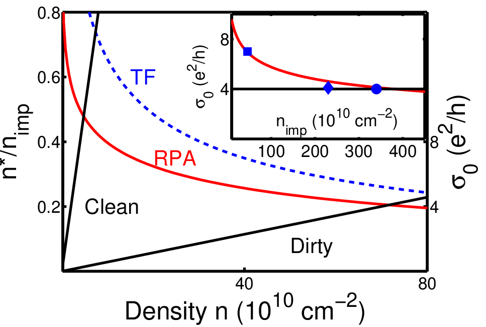
Based on estimates from surface probe measurements [7, 10], and consistent with earlier work both in graphene [4, 30] and in Si-MOSFETs [29, 40], we assume that the charged impurities lie in a plane at a distance from the graphene sheet and calculate the voltage fluctuations taking into account of screening using the RPA approximation. The screened voltage fluctuation is a function of and the carrier density ; a larger carrier density more effectively screens the charged impurities, while the potential fluctuations are larger for low carrier density. We include this effect self-consistently in our theory, where is both determined by and determines the screened impurity potential. Our theoretical results do not depend in any qualitative manner on the precise choice of , and one can develop relationships between the four experimental quantities (i.e. mobility, plateau width, minimum conductivity and shift in gate voltage) that are independent of . We emphasize that since a single parameter determines all four experimental quantities, we anticipate that our theory would be consistent with each of them to within a factor of 2. Comparison with representative samples from the Columbia, Manchester, and Maryland groups (see inset of Fig. 3 and note added at the end of this paper) shows agreement for the mobility and gate-voltage shift and agrees to within the expected factor of 2 with measurements of the plateau width and minimum conductivity.
We now proceed to calculate the Boltzmann transport conductivity. For 2D graphene, the semi-classical diffusive conductivity is given by
| (4) |
where are the spin and valley degeneracy factors and the mean free path , with the scattering time being given at by
| (5) |
where is the Fourier Transform of bare Coulomb potential at the transfer momentum . While the exact RPA dielectric function is known [41], for our purposes we can use the following simple approximate expression which allows for analytic calculations and provides results that are indistinguishable from the exact results (see Fig 2)
where , and solving the integrals exactly we find
| (9) | |||||
where for graphene on a SiO2 substrate, , and . Note that is positive and real for all . From this we derive a simple analytical expression for linear tail mobility in graphene
| (10) |
where and . Note that Eq. 10 depends only on the charged impurity scattering concentration , indicating that the only way to increase graphene mobility for fixed is to improve the sample quality. However, Eq. 9 also shows that mobility depends on the substrate dielectric constant , and therefore changing the underlying substrate from SiO2 to one with a higher dielectric constant would reduce , and would be another way to increase sample mobility. For example, changing the substrate to Hf02 () from SiO2 (), should enhance graphene mobility by a factor of 5.

We now calculate the statistics of the random voltage fluctuations significantly extending earlier numerical work [5] to incorporate analytically the non-linear screening of electrons and holes in a zero-gap situation, to find
| (11) | |||||
| (12) | |||||
where the superscript on indicates that we used the RPA Approximation, and is the exponential integral function. The voltage fluctuation result is shown in Fig. 2 comparing different approximation schemes used in the literature. The analytic result Eq. 12 is compared with a numerical evaluation of Eq. 11 using the exact dielectric function first reported in Ref. [41], as well as with the long-wavelength (also known as Thomas-Fermi) approximation [30], where for all , and the “complete screening” approximation [2, 5] that is valid only for , where . In the limit of large (i.e. ), both the Thomas-Fermi and the RPA result approach the complete screening limit of , that was previously obtained in Ref. [5]. The three approximations disagree in the small (or low density) limit where
| (13) |
and is Euler’s constant. Notice that for RPA, a combination of the small and large asymptotes span most of the density range. While these analytical asymptotes correctly describe the screened potential for most densities, it turns out, that the regime relevant to graphene experiments is the window where they do not work well, and the full functional form of shown in Eq. 12 needs to be used.
As discussed earlier, to determine the self-consistent residual density, we equate the average chemical potential to the fluctuation in the screened charged impurity induced potential as , and find
| (14) |
where the second expression for the impurity induced shift in voltage is determined from [5, 30]. Combining these results gives Eq A self-consistent theory for graphene transport.
Shown in the main panel of Fig. 3 are the results of the self-consistent procedure. The inset shows the value of the minimum conductivity and compares with the experimental results. These are the same three samples that were shown in Ref. [4] to compare the conductivity at high carrier density (far from the Dirac point) with a numerical Boltzmann theory, and here we show the low carrier density comparison near the Dirac point. Through Eq. 10, we have the high-density measurements directly giving , and this is the only parameter used to determine the minimum conductivity . Our results show that contrary to common perception, the graphene minimum conductivity is not universal, but that future cleaner samples will have higher values of . We emphasize that, in addition to explaining the value of and its dependence on the sample quality, our theory also naturally accounts for the width of the minimum conductivity plateau in agreement with experiments. For example, gives and plateau width .
We emphasize that the most important qualitative result of our theory is to introduce a realistic mechanism operational in all disordered graphene samples (i.e. in the presence of random charged impurities) which produce a plateau-like approximate non-universal minimum graphene conductivity at low induced carrier density. We obviously can not rule out other possible “universal mechanisms” which will lead to a “universal” minimum intrinsic graphene conductivity at the Dirac point in the clean limit, a situation beyond the scope of our theory. But the fact that the currently existing experimental data from three different groups exhibit non-universal minimum conductivity in approximate (within a factor of 2) agreement with our theory indicates that any intrinsic universal mechanism beyond our model may not yet be playing any role. We note however, that there have been recent theoretical [39, 42, 43] and experimental [44] work dealing with ballistic transport in mesoscopic graphene which show universal behavior in the regime where , where is the mean free path, and and are the sample width and length. Our theory does not apply in this zero disorder ballistic limit since our work is entirely built on the picture of diffusive transport through disorder induced electron-hole puddles.
In summary, we believe we have qualitatively and semi-quantitatively solved one of the main transport puzzles in graphene, namely, why the experimentalists see a conductivity minimum plateau and the extent to which this minimum conductivity is or is not universal. The theory developed here should only be taken as the first step toward a full quantitative theory of graphene transport, particularly at the lowest carrier densities. Many questions still remain open, although we believe that we have taken an important step in the right direction. In particular, the precise nature of transport at the charge neutral Dirac point can not be accessed by our self-consistent treatment which is valid only at finite doping away from charge neutrality. The percolation through electron and hole puddles becomes precisely equivalent at the Dirac point, and a purely percolative theory, not our self-consistent RPA-Boltzmann theory, would be necessary to understand the transport. We do, however, mention that the observed smooth behavior of conductivity as a function of gate voltage through the charge neutrality point indicates a lack of any dramatic phenomena at the Dirac point, and given that our theory is a good description of transport away from the Dirac point, it is conceivable that it remains quantitatively valid at the charge neutral point also. Given the great deal of current interest in graphene and the potential for graphene-based electronics applications, our transport theory of graphene not only furthers our understanding of this new material, but it provides essential insights on how to obtain higher mobility, which is necessary if graphene is to have serious technological impact as a new electronic material.
Acknowledgements.
This work is supported by the US-ONR, LPS-NSA, NSF-NRI and the Microsoft Project Q. It is a pleasure to thank M. Fuhrer, A. Geim, P. Kim and H. Stormer for sharing with us their experimental data. Note Added: After submission of this manuscript, there have been two experimental studies by Ref. [45] and Ref. [46] who find that our transport theory is in good agreement with experimental data taken over a wide range of charged impurity densities.References
- [1] Ando, T. (2006) J. Phys. Soc. Jpn. 75, 074716–074723.
- [2] Nomura, K. & MacDonald, A. H. (2007) Phys. Rev. Lett. 98, 076602–076606.
- [3] Cheianov, V. V. & Fal’ko, V. I. (2006) Phys. Rev. Lett. 97, 226801–226805.
- [4] Hwang, E. H., Adam, S., & Das Sarma, S. (2007) Phys. Rev. Lett. 98, 186806–186809.
- [5] Efros, A. L., Pikus, F. G., & Burnett, V. G. (1993) Phys. Rev. B 47(4), 2233–2243.
- [6] Novoselov, K. S., Geim, A. K., Morozov, S. V., Jiang, D., Zhang, Y., Katsnelson, M. I., Grigorieva, I. V., Dubonos, S. V., & Firsov, A. A. (2005) Nature 438, 197–200.
- [7] Novoselov, K. S., Geim, A. K., Morozov, S. V., Jiang, D., Zhang, Y., Dubonos, S. V., Grigorieva, I. V., & Firsov, A. A. (2004) Science 306, 666–669.
- [8] Yan, J., Zhang, Y., Kim, P., & Pinczuk, A. (2007) Phys. Rev. Lett. 98, 166802–166805.
- [9] Bostwick, A., Ohta, T., Seyller, T., Horn, K., & Rotenberg, E. (2007) Nature Physics 3, 36–40.
- [10] Ishigami, M., Chen, J. H., Cullen, W. G., Fuhrer, M. S., & Williams, E. D. (2007) Nano Lett. 7, 1643.
- [11] Martin, J., Akerman, N., Ulbricht, G., Lohmann, T., Smet, J. H., von Klitzing, K., & Yacobi, A. (2007) Preprint (arXiv:0705.2180v1 [cond-mat.mes-hall]).
- [12] Meyer, J. C., Geim, A. K., Katsnelson, M. I., Novoselov, K. S., Booth, T. J., & Roth, S. (2007) Nature 446, 60–63.
- [13] Bunch, J. S., van der Zande, A. M., Verbridge, S. S., Frank, I. W., Tanenbaum, D. M., Parpia, J. M., Craighead, H. G., & McEuen, P. L. (2007) Science 315, 490–493.
- [14] Chen, J. H., Ishigami, M., Jang, C., Fuhrer, M.S., Hines, D., & Williams, E. D. (2007) Adv. Mater. (2007) in press.
- [15] Heersche, H. B., Jarillo-Herrero, P., Oostinga, J. B., Vandersypen, L. M. K., & Morpurgo, A. F. (2007) Nature 446, 56–59.
- [16] Hill, E. W., Geim, A. K., Novoselov, K., Schedin, F., & Blake, P. (2006) IEEE Trans. Magn. 42, 2694–2696.
- [17] Lemme, M.C., Echtermeyer, T.J., Baus, M., & Kurz, H. (2007) IEEE Electron Device Letters 28, 282–284.
- [18] Huard, B., Sulpizio, J. A., Stander, N., Todd, K., Yang, B., & Goldhaber-Gordon, D. (2007) Phys. Rev. Lett. 98, 236803–236806.
- [19] Williams, J. R., DiCarlo, L., & Marcus, C. M. (2007) Science 317, 638–641.
- [20] Schedin, F., Geim, A. K., Morozov, S. V., Jiang, D., Hill, E. H., Blake, P., & Novoselov, K. S. (2007) Nature Materials 6, 652–655.
- [21] Han, M. Y., Ozyilmaz, B., Zhang, Y., & Kim, P. (2007) Phys. Rev. Lett. 98(20), 206805–206809.
- [22] Zhang, Y., Tan, Y-W, Stormer, H. L., & Kim, P. (2005) Nature 438, 201–204.
- [23] Fradkin, E. (1986) Phys. Rev. B 33(5), 3257–3262.
- [24] Ludwig, A. W. W., Fisher, M. P. A., Shankar, R., & Grinstein, G. (1994) Phys. Rev. B 50(11), 7526–7552.
- [25] Ziegler, K. (2006) Phy. Rev. Lett. 97, 266802–266806.
- [26] Aleiner, I.L. & Efetov, K.B. (2006) Phys. Rev. Lett. 97, 236801–236805.
- [27] Altland, A. (2006) Phys. Rev. Lett. 97, 236802–236806.
- [28] Ostrovsky, P. M., Gornyi, I. V., & Mirlin, A. D. (2006) Phys. Rev. B 74, 235443–235463.
- [29] Ando, T., Fowler, A. B., & Stern, F. (1982) Rev. Mod. Phys. 54, 437–672.
- [30] Galitski, V. M., Adam, S., & Das Sarma, S. (2007) Preprint (cond-mat/0702117).
- [31] Das Sarma, S. & Hwang, E. H. (2003) Phys. Rev. B 68(19), 195315–195324.
- [32] Ilani, S., Yacoby, A., Mahalu, D., & Shtrikman, H. (2000) Phys. Rev. Lett. 84(14), 3133–3136.
- [33] Stauffer, D. & Aharony, A. (2001) Introduction to percolation theory (Taylor and Francis, Philadelphia).
- [34] Das Sarma, S., Lilly, M. P., Hwang, E. H., Pfeiffer, L. N., West, K. W., & Reno, J. L. (2005) Phys. Rev. Lett. 94(13), 136401–136405.
- [35] Allison, G., Galaktionov, E. A., Savchenko, A. K., Safonov, S. S., Fogler, M. M., Simmons, M. Y., & Ritchie, D. A. (2006) Phys. Rev. Lett. 96(21), 216407–216411.
- [36] Tracy, L. A., Eisenstein, J. P., Lilly, M. P., Pfeiffer, L. N., & West, K. W. (2006) Solid State Commun. 137, 150–155.
- [37] Bardarson, J. H., Tworzydlo, J., Brouwer, P. W., & Beenakker, C. W. J. (2007) Phys. Rev. Lett. 99, 106801–106803.
- [38] Nomura, K., Koshino, M., & Ryu, S. (2007) Phys. Rev. Lett. 99, 146806–146806.
- [39] Katsnelson, M. I. (2006) Eur. Phys. J. B 51, 157–160.
- [40] Das Sarma, S. & Hwang, E. H. (2004) Phys. Rev. B 69, 195305–195320.
- [41] Hwang, E. H. & Das Sarma, S. (2007) Phys. Rev. B 75(20), 205418–206424.
- [42] Tworzydło, J., Trauzettel, B., Titov, M., Rycerz, A., & Beenakker, C. W. J. (2006) Phys. Rev. Lett. 96(24), 246802–246806.
- [43] Fertig, H. A. & Brey, L. (2006) Phys. Rev. Lett. 97(11), 116805–116809.
- [44] Miao, F., Wijeratne, S., Zhang, Y., Coskun, U., Bao, W., & Lau, C.N. (2007) Science 317, 1530–1533.
- [45] Tan, Y.-W., Zhang, Y., Bolotin, K., Zhao, Y., Adam, S., Hwang, E. H., Das Sarma, S., Stormer, H. L., & Kim, P. (2007) Preprint(arXiv:0707.1807v1 [cond-mat.mes-hall]).
- [46] Chen, J. H., Jang, C., Fuhrer, M. S., Williams, E. D., & Ishigami, M. (2007) Preprint(arXiv:0708.2408v1 [cond-mat.mes-hall]).